requirements elicitation for complex systems theory and practice

code design for dependable systems theory and practical applications
... V and for all scalar c F cðu þ vÞ ¼ cu þ cv for all u, v V and for all scalar c F ða þ bÞv ¼ av þ bv for all v V and for all scalars a, b F ðabÞv ¼ aðbvÞ, 1v ¼ v, and 0v ¼ for all v V and for ... disks and tapes, logic circuits and systems, data entry systems, and distributed storage systems Also new classes of matrix codes, such as error locating codes, spotty byte error control codes, and ... the codes for some specific systems, namely mass memories such as magnetic tapes and disks, logic circuits and systems, data entry systems, and distributed storage systems Chapter 11 covers the...
Ngày tải lên: 03/06/2014, 01:48

Mosfet Modeling for VLSI Simulation: Theory And Practices by N. Arora pot
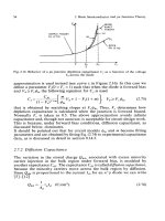
... quantity and is plotted upward on the energy-band diagram If E, and E, are the energy levels for the lower edge of the conduction band and upper edge of the valence band respectively, then the band ... energy bands is often referred to as the forbidden band or forbidden gap Although the energy is a complex function of momentum in three dimensions and there are so many energy levels, and so many ... Semiconductor and p n Junction Theory FREE ELECTRON (-) HOLE (+I Fig 2.1 Energy band diagram of a semiconductor (silicon) separate bands of allowed energies, called the valence band and the conduction band...
Ngày tải lên: 27/06/2014, 05:20

MOSFET MODELING FOR VLSI SIMULATION Theory and Practice docx
... quantity and is plotted upward on the energy-band diagram If E, and E, are the energy levels for the lower edge of the conduction band and upper edge of the valence band respectively, then the band ... energy bands is often referred to as the forbidden band or forbidden gap Although the energy is a complex function of momentum in three dimensions and there are so many energy levels, and so many ... Semiconductor and p n Junction Theory FREE ELECTRON (-) HOLE (+I Fig 2.1 Energy band diagram of a semiconductor (silicon) separate bands of allowed energies, called the valence band and the conduction band...
Ngày tải lên: 27/06/2014, 18:20

MOSFET MODELING FOR VLSI SIMULATION - Theory and Practice Episode 1 potx
... catalogue record for this book is available from the British Library MOSFET MODELING FOR VLSI SIMULATION Theory and Practice International Series on Advances in Solid State Electronics and Technology ... editors and this monograph volume’s copy editor Mr Tjan Kwang Wei at Singapore, led by Dr Yubing Zhai at New Jersey, for their and her timely efforts, and Professor Kok-Khoo Phua, Founder and Chairman ... (Corporate Consultant) and Dr Llanda Richardson (Consultant )for their encouragement and assistance in writing this book I am deeply indebted to Dr F Fox, Dr D Ramey, and Mr K Mistry for their excellent...
Ngày tải lên: 13/08/2014, 05:22

MOSFET MODELING FOR VLSI SIMULATION - Theory and Practice Episode 2 ppt
... semiconductor and silicon are used interchangeably 2 Basic Semiconductor and pn Junction Theory 22 CONDUCTION BAND - eV(P) + €, 7- - E d Eg=1-12eV I L VALENCE BAND EV t VALENCE BAND (a) (b) CONDUCTION BAND ... Semiconductor and p n Junction Theory 38 Similarly for holes we have (2.38b) where R, and G are recombination and generation rates for holes These , equations are called continuity equations for electrons ... Vd); v is positive for forward bias and negative for d reuerse bias If the applied forward voltage is exactly equal to the built-in voltage, there will be no barrier and therefore, there will be...
Ngày tải lên: 13/08/2014, 05:22
MOSFET MODELING FOR VLSI SIMULATION - Theory and Practice Episode 3 docx
... I , and I , for the two different structures as a function of voltage and knowing A,, P a ,A , and P, for the two structures, we can calculate I,,,, and Iperi using Eq (2.81) respectively for ... use of (2.76) for Qdif and Id is given by Eq (2.82) Using Eqs (2.74) and (2.75) for Cj we get vd ' Fc($bi (2.86) Basic Semiconductor and p n Junction Theory 64 The variables F,,F, and F3 are F, ... temperature SPICE assumes E , = 1.11 eV for silicon, 0.67 eV for Germanium, and 0.69 eV for SBD The temperature exponent factor p equals for silicon and germanium while for SBD its value is From Eq (2.91),...
Ngày tải lên: 13/08/2014, 05:22

MOSFET MODELING FOR VLSI SIMULATION - Theory and Practice Episode 4 doc
... Structure and Operation (primary substrate p-type for nMOST and n-well for pMOST) or a p-well process (primary substrate n-type for pMOST and p-well for nMOST) Another alternative is to form two ... between the contact via and the channel region, p , is the sheet resistance per square (n/o) and W is device width For a typical pm CMOS technology, p , = 30 and R / O for n+ and p + regions, respectively ... device behavior For increased current drive and hence circuit speed a large W and small L is required It is important to understand what device L and W stand for from the modeling point of view 3.7.1...
Ngày tải lên: 13/08/2014, 05:22

MOSFET MODELING FOR VLSI SIMULATION - Theory and Practice Episode 5 ppsx
... solve for the MOS capacitance at flat band, called thepat band capacitance C f b ,we need to use Eq (4.48) for Q , or Eq (4.57) for C, For < we have e - + s >> e C + f > e - + f + sand therefore, ... expression for Q, that is valid for all the regimes of device operation by including both the holes and electrons and thus solving the Poisson Eq (2.41) Using Eqs (4.33) for n and p and noting ... curve for a uniformly doped substrate is straightforward as discussed in section 4.3 However, for a nonuniformly doped substrate one needs to solve Poisson’s equation numerically using the nonuniform...
Ngày tải lên: 13/08/2014, 05:22
MOSFET MODELING FOR VLSI SIMULATION - Theory and Practice Episode 6 pptx
... charge and hence threshold voltage However, such complex models are not suitable for use in circuit simulators For this reason they are not discussed here and details of the equations for Qb and ... (5.37) Solving Eqs (5.38) and (5.39) for N,, and using Eq (5.36) for X , , yields (5.40) where q5i is given by Eq (5.35) This value of N , , is used for N , in Eq (5.29) for the body factor term ... N,, becomes a function of back bias, and therefore y is no longer a constant but is bias dependent For a uniformly doped substrate N , equals N , , and therefore Eq (5.40) gives N,, = N , Thus,...
Ngày tải lên: 13/08/2014, 05:22

MOSFET MODELING FOR VLSI SIMULATION - Theory and Practice Episode 7 doc
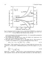
... (a), (b) and (c) are for channel implanted devices, curve (d) is for uniformaly doped device Although both curves (b) and (c) are for enhancement devices, curve (b) has higher t0,(300A), and lower ... capacitance and is obtained by differentiating d the bulk charge Qb For example, for a uniformly doped substrate, we can write Cd = Y C O X 2d+Ti,b' (5.110) On the other hand, Yang and Chaterjee's ... sequently Tot,, (a) and (b) (Figs 5.31 and 5.32) which are for Vsb = V and V, respectively n-Channel Devices (nMOST) For n-channel enhancement devices (' n polysilicon gate and p-substrate) &D,,/dT...
Ngày tải lên: 13/08/2014, 05:22

MOSFET MODELING FOR VLSI SIMULATION - Theory and Practice Episode 8 potx
... 4, by q5s, and have made use of Eq (6.23) for y and Eq (6.22) for Vq! Remembering that Vcb(y 0) = V b and Vcb(y L) = = , = V,b+ V,,, the inversion charge Q i s and Qid at the source and drain ... mobility model is &e;t (6.143) where d1 and 8, are fitting parameters, and m = for electrons and m = for holes At lower fields where fixed oxide charge scattering and Coulomb scattering are important, ... value lies between and 0.5 and represents the contribution to the field due to drain voltage The exponent v is approximately 0.25 for n-channel and 0.15 for p-channel devices [SO] For devices in...
Ngày tải lên: 13/08/2014, 05:22
MOSFET MODELING FOR VLSI SIMULATION - Theory and Practice Episode 9 potx
... Eqs (6.142), (6.174) and (6.204) for p,, Vds,, and ld, respectively The corresponding I d , - Vd, and I,, - Vgscharacteristics for n-channel device are shown in Figures 6.34b and 6.34c, respectively ... device and circuit performance’, IEEE Trans Electron Devices, ED-31, pp 1386-1396 (1984) [90] B Hoefflinger, H Sibbert, and G Zimmer, ‘Model and performance of hot electron MOS transistor for VLSI’, ... this is true only for a uniformly doped substrate For practical MOSFET’s which are nonuniformly doped, y is bias dependent as was discussed in Chapter Therefore, proper y value and derivative need...
Ngày tải lên: 13/08/2014, 05:22

MOSFET MODELING FOR VLSI SIMULATION - Theory and Practice Episode 10 pot
... following empirical relation for was observed for long channel and thick gate oxide devices [17] x = 0.22to'13Xf'Z For to, < 15081 and (8.15) L < 0.5 pm, Eq (8.15) for has been modified as [lo] ... function of V,, at V,, = 4.6 and 3.8 V and V,, = OV for a typical MOSFET Circles are experimental points for an n-channel LDD device ( L = 0.77 pm and to, = 150A).Solid, dashed and dotted lines are different ... technology dependent fitting parameter and is different is for standard and LDD devices Further, results from MINIMOS simulations also indicate that for a given to, and X j , the effective ionization...
Ngày tải lên: 13/08/2014, 05:22
MOSFET MODELING FOR VLSI SIMULATION - Theory and Practice Episode 11 pdf
... quasi-static application of Eq (8.35) for nMOST [8], [41] and Eq (8.37) for pMOST [47] Thus, for example, zACfor nMOST is given by (8.38) where T is the full cycle time, I , and I d are the currents at ... injection before and after stress (After Hu et al [ ] ) "'"0.0 1.0 2.0 3.0 DRAIN VOLTAGE, , V , L-0 50 (V) Fig 8.13 I,, - V,, characteristics of a nMOST ( L = 1.2pm and to, = 200@ before and after ... pronounced for large back bias V,b and thin gate oxides (tax < loo& In fact, interface generation due to hot holes and hot electrons has been reported for 0.25 pm pMOST leading to a reduction in g m and...
Ngày tải lên: 13/08/2014, 05:22

MOSFET MODELING FOR VLSI SIMULATION - Theory and Practice Episode 12 ppt
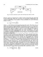
... (4.63) and (4.64) as (9.19) Although Eqs (9.18) and (9.19) are derived for uniform substrate doping, they remain valid for the case of nonuniform doping These are the basic equations for measuring ... Combining Eqs (2.15) and (4.74) and solving for the substrate concentration N yields (9.13) where A, is the MOS capacitor gate area This is a transcendental equation for N and therefore must be solved ... condition from the following equation (9.10) where the + and - signs are for n- and p-substrate, respectively, and c h f o and CLfo are values of c h f and C k , respectively, at V, = V,, Extract C,,...
Ngày tải lên: 13/08/2014, 05:22

MOSFET MODELING FOR VLSI SIMULATION - Theory and Practice Episode 13 ppsx
... W = W,,, - A W [cf Eq (3.33)] It is the L and W and not L, and W, which are used for modeling MOSFET devices (cf section 3.7) This in turn requires AL and A W to be known In this section we will ... proposed by Terada and Muta 1601, was reformulated by Chern et al [61] and later slightly modified by many others [62]-[68] It is the most commonly used method for determining AL and has become widely ... = 01 - (9.66) 2(801 - ) where Q and d2 are the values for (do/po R,) for the devices with channel respectively length L,, and Lm2, In a method proposed by Suciu and Johnston [79], the quantity...
Ngày tải lên: 13/08/2014, 05:22

MOSFET MODELING FOR VLSI SIMULATION - Theory and Practice Episode 14 potx
... I,, and gd,, we will have (10.57) where W, and W, are the relative weights for the current and conductance respectively, wi is the weight for each data point (current or conductance) and r12(p )and ... effort for calculating the Hessian H in order to solve for Ap In general, the Hessian matrix H is difficult to solve with sufficient accuracy For this reason approximations are often used for ... methods for estimating the Jacobian This is because the model equations are usually complex function of the model parameters, and therefore the task of deriving partial derivatives becomes tedious and...
Ngày tải lên: 13/08/2014, 05:22
MOSFET MODELING FOR VLSI SIMULATION - Theory and Practice Episode 15 doc
... mean and standard deviation for each of the model parameters obtained from different dice and wafers Once the mean pi and the standard deviation si for each parameter p i is known, a test for ... creation of W C F for circuit simulation and design basically consists of two parts: (1) extracting model parameters for different length and width devices for each die and wafer, and (2) determining ... parameters, for threshold voltage (V,,, d f , y , K , and v ] ) and for drain current (Po, U o , U , and n) However, parameters ( v ] , Po, U o , U , and n) depend on bias voltages Vd, and V,, as...
Ngày tải lên: 13/08/2014, 05:22

MOSFET MODELING FOR VLSI SIMULATION - Theory and Practice Episode 16 doc
... distributed and vice versa The density plot for a bivariate normal distribution with standarized variables x and y for p = 0.5 and 0.9 are shown in Figure H.2 Note that the paths of x and y values ... ofStatistics’, Chapman and Hall, New York, 1987 [16] R E Walpole and R H Myers, Probability and Statisticsfor Engineers and Scientists, McGraw Hill, New York, 1976 [17] C W Helstrom, Probability and Stochastic ... Chapman and Hall, New York, 1987 [2] R E Walpole and R H Myers, Probability and Statisticsfor Engineers and Scientists, McGraw Hill, New York, 1976 [3] [3] C W Helstrom, Probability and Stochastic...
Ngày tải lên: 13/08/2014, 05:22