MOSFET MODELING FOR VLSI SIMULATION - Theory and Practice Episode 15 doc
MOSFET MODELING FOR VLSI SIMULATION - Theory and Practice Episode 15 doc
... manage- able form, if the following substitutions are made (1 1.26a) 538 11 SPICE Diode and MOSFET Models s - 1 0-4 u 1 0-5 3 1 0-6 0 U z U U 0 I %= 8.99 1 0-1 4 A r,= 15. 88R ... IEEE Int. Conf. on Computer-Aided Design, ICCAD-84, pp. 18 4-1 51 (1984). [13] S. L. Wong and C. A. T. Salama, ‘Improved simulation of p- and n-channel MO...
Ngày tải lên: 13/08/2014, 05:22
MOSFET MODELING FOR VLSI SIMULATION - Theory and Practice Episode 3 docx
... + + pMOST - - - + terminal voltages as drain-source voltage Vds( = V, - VJ, gate-source voltage V,,( = V, - V,), and bulk-source voltage vb,( = vb - Vs). For normal DC ... 2 Basic Semiconductor and pn Junction Theory The variables F,,F, and F3 are F, =- *bi [l -( 1 - F,)&apos ;-& quot;] (1 -4 F2 = (1 - F,...
Ngày tải lên: 13/08/2014, 05:22

MOSFET MODELING FOR VLSI SIMULATION - Theory and Practice Episode 4 doc
... Structure and Operation ~i 1; L 6i! - - - - - - - - - Fig. 3.3 1 Cross-section showing overlap capacitances between the source/drain and the gate which give rise to C,,, and CGDo ... order expression for Rsp, based on the assumption of uniform doping 128 4 MOS Capacitor I- -t > O O+ -0 .6 1 A1 (p-Si n+ Po~y(p-si) -o...
Ngày tải lên: 13/08/2014, 05:22

MOSFET MODELING FOR VLSI SIMULATION - Theory and Practice Episode 7 doc
... model for drain-induced barrierlowering and drain-induced high electric field in a short-channel MOSFET , Solid-State pp. 11 8-1 27 (1989). Electron., 30, pp. 50 3-3 11 (1987). [78] Y. Omura and ... (a) and (b) (Figs. 5.31 and 5.32) which are for Vsb = 3 V and 0 V, respectively. n-Channel Devices (nMOST). For n-channel enhancement devices (n' polysil...
Ngày tải lên: 13/08/2014, 05:22

MOSFET MODELING FOR VLSI SIMULATION - Theory and Practice Episode 16 doc
... effect, 15 9-1 60 accumulation, 149 deviation from ideal, 15 6-1 59 depletion, 15 0- 152 deep depletion, 155 inversion, 152 high frequency, 154 low frequency, 153 measurement of, 41 8-4 21 Channel ... small-signal capacitances, 14 9-1 50 in MOSFET, 171, 33 2-3 33, 347 Avalanche effect, 52 Back gate bias, 78 Band bending, 12 5-1 27 Band diagram, 16...
Ngày tải lên: 13/08/2014, 05:22

MOSFET MODELING FOR VLSI SIMULATION - Theory and Practice Episode 1 potx
... Frequency C-V Plot 153 4.3.2 High Frequency C-V Plot 154 4.3.3 Deep Depletion C-V Plot 155 4.4 Deviation from Ideal C-V Curves 156 4.5 Anomalous C-V Curve (Polysilicon Depletion Effect) 159 4.6 ... transistors and related devices’, IEEE Trans. Electron Devices, ED-23, pp. 65 5-6 60 (1976); J. D. Meindl, ‘Ultralarge scale integration’, ibid, ED-31, pp. 155 5-1 561 (1984)....
Ngày tải lên: 13/08/2014, 05:22

MOSFET MODELING FOR VLSI SIMULATION - Theory and Practice Episode 2 ppt
... 1982 and given in many textbooks) by as much as 50% for boron doped p-type silicon. For phosphorous doped n-type silicon the difference is only 157 4. Curves for n-type are lower than p-doped ... conditions is given by the Fermi-Dirac At 77K ni for silicon is -1 0-2 0cm-3, while at 400K its value is -1 O'*~m-~ 28 2 Basic Semiconductor and pn Junc...
Ngày tải lên: 13/08/2014, 05:22

MOSFET MODELING FOR VLSI SIMULATION - Theory and Practice Episode 5 ppsx
... df Qh Y <h VTO nMOST p-type - +- +++ pMOST n-type - -+ - (for metals and n+ polysilicon gate) - - (for metals and n+ polysilicon gate) + (for p+ polysilicon gate) (tax ... operation for a p-type substrate, N, = 5.1 015 cm- ’, to, = 300 A, and V,, = 0 V 4.2 MOS Capacitor at Non-Zero Bias 143 Using Eq. (4.29) f...
Ngày tải lên: 13/08/2014, 05:22
MOSFET MODELING FOR VLSI SIMULATION - Theory and Practice Episode 6 pptx
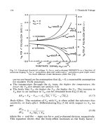
... >" ;- I 5 0.4 lY I bO.3 195 1'1'1'1'1~1'1'1~ I - Nb = 2 X 10'"cm-3 - - - - - W=20 m - f"\L "A&ING - I I 1 ... both pMOST and nMOST devices, a general expression for the threshold voltage can be written as (5.63) where the + and - signs are for n- and p-chan...
Ngày tải lên: 13/08/2014, 05:22

MOSFET MODELING FOR VLSI SIMULATION - Theory and Practice Episode 8 potx
... form that at first glance appears different. 6.7 Short-Geometry Models 3 - 2- - a 9- W- (7 5 9 1.75 Q t- 6 !I 3 t- 6 fJY 0.5 293 I = 1.31 x 10⁴V/cm a= 1.13 0 - ... and is often neglected. For p-channel devices improves the current-voltage data fit. The SPICE MOSFET Levels 3 and 4 models use 0,=0 in Eq. (6 .153 ) for both p- and...
Ngày tải lên: 13/08/2014, 05:22
- building software for simulation theory and algorithms with applications
- building software for simulation theory and algorithms with applications in c
- english grammar theory and practice for beginners
- building software for simulation theory and algorithms
- summary and final recommendations for theory and practice