english grammar theory and practice for beginners

Cambrige University Press English Grammar in Use-Reference and Practice for Intermediate Students
Ngày tải lên: 05/10/2012, 08:22

Báo cáo hóa học: " Our vision for this new SpringerOpen Access journal, Psychology of Well-Being: Research, Theory and Practice, is to promote a distinctly eclectic approach to investigating well-being. When the prospect of " pdf
... by pockets of poorly informed practice. Professional, evidence-based practice for enhancing well- being is now more feasible and this means that the credibility, value and longevity of well-being ... and incorporate the latest research findings into their practice, helping to narrow the gap betwe en science and practice. This scientist-practitioner partnership is especially important for ... Dordrecht, The Netherlands: Reidel. doi:10.1186/2211-1522-1-1 Cite this article as: Vella-Brodrick and Rickard: Editorial. Psychology of Well-Being: Theory, Research and Practice 2011 1:1. Submit...
Ngày tải lên: 21/06/2014, 06:20
Adaptive Techniques for Dynamic Processor Optimization Theory and Practice by Alice Wang and Samuel Naffziger_2 doc
... “Limits to Performance Spread Tuning Using Adaptive Voltage and Body Biasing,” International Sympo- sium on Circuits and Systems, pp. 5–8, May 2005. [3] J. T. Kao, M. Miyazaki, and A. P. Chandrakasan, ... current is due to band-to-band tunneling in the presence of high electric field and traps in the band gap. If the electric field is high enough, carriers can simply tunnel across the band gap. However, ... Techniques for SH4,” Short Course on Physical Design for Low Power, High Performance Microprocessor Circuits, 2001 Symposium on VLSI Circuits, 2001. [17] D. Scott, S. Tang, S. Zhao, and M. Nandakumar,...
Ngày tải lên: 21/06/2014, 22:20

Adaptive Techniques for Dynamic Processor Optimization Theory and Practice by Alice Wang and Samuel Naffziger_3 doc
... Power and Frequency Tuning The ultimate use of the AVS and ABB schemes is for performance tuning with performance being the optimal combination of frequency and power, i.e. the lowest power for ... power-performance trade-offs and leakage reduction factors with AVS and ABB. Each ring-oscillator uses minimum-sized standard-cell inverters as delay elements and a nand-2 gate for enabling ... Figure 2.5 Frequency scaling and tuning for the 65nm LP-CMOS ringo. Let us now investigate the frequency-scaling and tuning ranges offered by AVS and ABB in 65nm LP-CMOS. For this purpose, we determined...
Ngày tải lên: 21/06/2014, 22:20
Adaptive Techniques for Dynamic Processor Optimization Theory and Practice by Alice Wang and Samuel Naffziger_4 pptx
... scaling and adaptive body bias are useful for power and delay tuning in the state-of-the-art CMOS technologies. We observe the benefits of AVS primarily for low power and of ABB for performance ... both the active and the standby modes and raises V TH by 0.25V in the standby mode. Chapter 2 Technological Boundaries of Voltage and Frequency Scaling 45 based on voltage and frequency ... previous results for compensating process-dependent frequency and leakage spread. The values for frequency, power supply voltage, and leakage current are plotted for ref- erence and tuned process...
Ngày tải lên: 21/06/2014, 22:20
Adaptive Techniques for Dynamic Processor Optimization Theory and Practice by Alice Wang and Samuel Naffziger_6 pdf
... reduced, and forward body bias (in this example, NMOS forward body bias) can be applied to further increase the performance. This combination reduces the guardband needed for maximum temperature and, ... levels for correct functionality. 0 0.05 0.1 0.15 0.2 0 0.05 0.1 0.15 0.2 V IN−NAND , V OUT−NOR V OUT−NAND , V IN−NOR NAND NOR Figure 5.3a Butterfly plot of functional NAND and NOR ... power for the FBB design at the same clock frequency. When the adder is put into standby mode, ZBB is used for the core, and this results in a leakage reduction of 2×. Total power savings for...
Ngày tải lên: 21/06/2014, 22:20
Adaptive Techniques for Dynamic Processor Optimization Theory and Practice by Alice Wang and Samuel Naffziger_7 potx
... References [1] V. Gutnik and A. Chandrakasan, “Embedded power supply for low-power DSP,” IEEE Trans. VLSI Syst., vol. 5, no. 4, pp. 425–435, Dec. 1997. [2] A. Sinha and A. Chandrakasan, “Dynamic ... DD DDBAT P N V VV − = τ τ (5.4) where τ N and τ P are the NMOS and PMOS ON-times and V BAT is the bat- tery voltage. Thus, by fixing τ P , the values of τ N for specific load voltages can be predetermined. ... Delivery for U-DVS Systems 121 [11] B. Zhai, S. Hanson, D. Blaauw, and D. Sylvester, “Analysis and mitigation of variability in subthreshold design,” IEEE Intl. Symp. on Low Power Elec- tronics and...
Ngày tải lên: 21/06/2014, 22:20
Adaptive Techniques for Dynamic Processor Optimization Theory and Practice by Alice Wang and Samuel Naffziger_9 pot
... essentially an FET wire; and NAND and NOR gate paths consisting of a series of 4-high NAND and 3-high NOR gates respectively. Simulations were performed at two frequencies, F and F/3 where F was ... flow is shown for a large-scale integrated circuit. Emphasis is placed on the development of the target performance and testing to ensure that performance is met. Chapter 7 Sensors for Critical ... (7.12), and (7.25) in Equation (7.8) gives () ⎭ ⎬ ⎫ ⎩ ⎨ ⎧ ++ + = loadwwsource dd CTRC w TR anD α α . (7.28) The variables α d and α w are the temperature coefficients for the driver and wire...
Ngày tải lên: 21/06/2014, 22:20
Adaptive Techniques for Dynamic Processor Optimization Theory and Practice by Alice Wang and Samuel Naffziger_12 ppt
... generated for the 45 nm node by the Predictive Technology Model Nano-CMOS tool [17]. Values from the 2005 International Technology Roadmap for Semiconductors were used for supply and threshold ... Gordon, and M. Horowitz, “Supply and threshold voltage scaling for low power CMOS,” IEEE Journal of Solid-State Circuits, Volume 32, Issue 8, August 1997. [7] S. Rangan, N. Mielke and E. Yeh, ... for microarchitects as technology scaling continues and more and more increasingly ill-defined transistors are placed on each die. Process variations during fabrication result in a nonuniformity...
Ngày tải lên: 21/06/2014, 22:20
Adaptive Techniques for Dynamic Processor Optimization Theory and Practice by Alice Wang and Samuel Naffziger_13 pdf
... propagation. To speed them up requires consider- able effort, and hence hardware, and hence energy is typically expended in fast carry logic of some form. This ensures that the critical path – propagating ... propagation distances are comparatively rare; the effort, hardware, and power are expended on something which is rarely used. Given random operands, the longest carry chain in an N-bit adder is ... processor’s ALU operation which typically may include options to MOVE, AND, ADD or MULTIPLY operands. A MOVE is a fast operation and an AND, be- ing a bitwise operation, is a similar speed. ADDs, however,...
Ngày tải lên: 21/06/2014, 22:20
Adaptive Techniques for Dynamic Processor Optimization Theory and Practice by Alice Wang and Samuel Naffziger_14 pptx
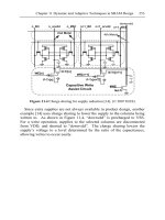
... cache sleeping and methods for regulating the sleep voltage, as well as schemes for taking the cache into and out of sleep are discussed. Finally, the chapter examines the yield and reliability, ... can provide benefits and is another tool available to the designer. Figure 10.7 Pipeline collapsing and losing latch stage. Figure 10.8 Pipeline expanding and reinstating latch ... simultaneously optimize for both read and write margins in the same operation, as needed in a column-multiplexed design. Therefore, row- based voltage manipulation tends to be more suitable for non-column- multiplexed...
Ngày tải lên: 21/06/2014, 22:20

Adaptive Techniques for Dynamic Processor Optimization Theory and Practice by Alice Wang and Samuel Naffziger_17 pot
... P max Large Guardband for Power measurment variability Small Guardband for Test environment issues Adaptive Op. Point Figure 12.18 Comparison of operating point with and without adaptation. ... ISBN 978-0-387-25737-2, 2005 Statistical Analysis and Optimization for VLSI: Timing and Power Ashish Srivastava, Dennis Sylvester, and David Blaauw ISBN 978-0-387-26049-9, 2005 Chapter ... standpoint, both analog and architectural designs require similarly sized guard-bands (Adaptive Op. Point, Figure 12.18) to guarantee power stays within limits. Because of issues in testing and...
Ngày tải lên: 21/06/2014, 22:20

MOSFET MODELING FOR VLSI SIMULATION Theory and Practice docx
... Consultant) and Dr. Llanda Richardson (Consultant) for their encouragement and assistance in writing this book. I am deeply indebted to Dr. F. Fox, Dr. D. Ramey, and Mr. K. Mistry for their ... editors and this monograph volume’s copy editor Mr. Tjan Kwang Wei at Singapore, led by Dr. Yubing Zhai at New Jersey, for their and her timely efforts, and Professor Kok-Khoo Phua, Founder and ... electrons in the conduction band and holes in the valence band is represented by the effective masses of the electrons (m:) and holes (m;) respectively, and by the equivalent positive...
Ngày tải lên: 27/06/2014, 18:20

A framework of knowledge management systems issues and challenges for theory and practice
... experience, values, contextual information and expert insight that provide a framework for evaluation and incorporating new experiences and information” (Davenport and Prusak 1997, p. 5). Prior ... what information will be requested, who will request the information, who will supply the information, and when and how the information will be used. This makes determining requirements for KMS development ... Ties: A Network Theory Revisited,” in Social Structure and Network Analysis, P. Marsden and N. Lin (eds.), New York: John Wiley and Sons, 1982, pp. 105-130. Hansen, M. T., Nohria, N., and Tierney,...
Ngày tải lên: 30/06/2014, 21:16
Adaptive Techniques for Dynamic Processor Optimization Theory and Practice Episode 2 Part 5 pot
... cache sleeping and methods for regulating the sleep voltage, as well as schemes for taking the cache into and out of sleep are discussed. Finally, the chapter examines the yield and reliability, ... Garside Unfortunately, this is not the whole story because there is an overhead in detecting the carry completion and, in any case, ‘real’ additions do not use purely random operands [13]. ... can provide benefits and is another tool available to the designer. Figure 10.7 Pipeline collapsing and losing latch stage. Figure 10.8 Pipeline expanding and reinstating latch...
Ngày tải lên: 06/08/2014, 01:21
Adaptive Techniques for Dynamic Processor Optimization Theory and Practice Episode 2 Part 6 ppt
Ngày tải lên: 06/08/2014, 01:21

Adaptive Techniques for Dynamic Processor Optimization Theory and Practice Episode 2 Part 7 potx
Ngày tải lên: 06/08/2014, 01:21

Adaptive Techniques for Dynamic Processor Optimization Theory and Practice Episode 2 Part 8 pot
Ngày tải lên: 06/08/2014, 01:21

MOSFET MODELING FOR VLSI SIMULATION - Theory and Practice Episode 1 potx
Ngày tải lên: 13/08/2014, 05:22