self aligned poly gate cmos transistors 376
Self aligned doping profiles in nanoscale silicon structures
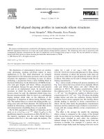
... to an oxidizing ambient we can obtain a selfaligned pnp structure We demonstrate the feasibility of this self- aligning method by fabricating so called self- switching devices [6] in silicon The ... conduction type of the channel has changed from p-type to n-type, and consequently, the device has a self- aligned pnp doping profile from drain to channel to source The quantitative doping concentrations ... fabricating so called self- switching devices [6] in silicon The device is essentially a lateral double gate FET connected as a diode A top-view SEM image of such a device is shown in Fig 2(a) Depending...
Ngày tải lên: 16/03/2014, 15:20
Self aligned silicon quantum wires on ag(1 1 0)
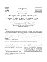
... about 30 nm in length, are formed at the early stages of the deposition at RT, apparently from the self- assembly of nanodots, which appear as their swiftly diffusing building blocks The density of ... at RT; as will be seen later it can be reduced upon mild annealing All these NWs are perfectly aligned along the [À1 0] direction of the Ag(1 0) surface, showing rounded protrusions (Fig 1(b)), ... exclude tip convolution effects Upon mild annealing at 230 °C for about 10 they further markedly elongate, keeping the same narrow width, well beyond 100 nm, as shown in Fig 2; in this case their density...
Ngày tải lên: 16/03/2014, 15:36

Báo cáo hóa học: " A Novel Self-aligned and Maskless Process for Formation of Highly Uniform Arrays of Nanoholes and Nanopillars" pot
... demonstrated a novel maskless and self- aligned sub-wavelength photolithography technique for forming highly uniform arrays of nanoholes and nanopillars The technique utilizes the self- assembled property ... an AZ300 MIF developer A large area of HCP monolayer of silica or PS spheres was formed by the self- assembled drop-coating method [10] To form a good monolayer of micro- and nanospheres on photoresist, ... sizes Nanoscale Res Lett (2008) 3:123–127 Similar simulation results could also be obtained for polystyrene (PS) spheres FWHM of the light intensity is a good measure of the photoresist exposure,...
Ngày tải lên: 21/06/2014, 22:20

Self aligned source and drain contact engineering for high mobility III v transistor
... 166 6.2.1 Self- Aligned NiGeSi Metallization for GaAs Planar n-MOSFETs 166 6.2.2 Self- Aligned Ni-InGaAs Contacts for InGaAs Planar n-MOSFETs 166 6.2.3 InGaAs FinFETs with Self- Aligned Ni-InGaAs ... n-MOSFETs is usually non -self- aligned with respect to the gate stack, unlike the self- aligned salicidation process in Si MOSFETs [2.24] A spacing between the contact metal and the gate stack leads to ... n-MOSFET with self- aligned NiGeSi contacts, gate length of 500 nm, and gate width of 100 μm, showing good transfer characteristics (b) ID-VD plot of the same device at various gate overdrive...
Ngày tải lên: 09/09/2015, 10:14

Schottky barrier engineering for contact resistance reduction in nanoscale CMOS transistors
... improvement of metal gate CMOS technologies,” VLSI Symp Tech Dig., pp 63-64, 2001 [1.4] Y.-T Hou, M.-F Li, T Low, and D.-L Kwong, “Metal gate work function engineering on gate leakage of MOSFETs,” ... scaling led approach to drive current enhancement for 22-nm CMOS technology and beyond This is an even bigger issue in multiple -gate transistors (for example FinFETs) which are slated for introduction ... materials include those used in the gate stack to enhance COX and hence drive current without adversely affecting gate leakage (high-κ dielectric and metal gate [1.3]-[1.6]), those used in the...
Ngày tải lên: 14/09/2015, 08:26

Báo cáo hóa học: " Organic electrochemical transistors based on a dielectrophoretically aligned nanowire array" pptx
... performance electrolyte gated carbon nanotube transistors Nano Lett 2002, 2:869 Alam MM, Wang J, Guo Y, Lee SP, Tseng HR: Electrolyte gated transistors based on conducting polymer nanowire junction ... electrochemical transistors, which consisted of two Au electrodes connected by CNT-Nafion nanowires and a remote Ag/ AgCl gate electrode immersed in an electrolyte droplet The electrochemical transistors ... thin-film transistor-driven polymer dispersed liquid crystal display on flexible polymeric substrates Appl Phys Lett 2002, 80:1088 Bartic C, Borghs G: Organic thin-film transistors as transducers...
Ngày tải lên: 21/06/2014, 04:20

Báo cáo hóa học: " Binary Mixtures of SH- and CH3-Terminated Self-Assembled Monolayers to Control the Average Spacing Between Aligned Gold Nanoparticles" doc
... lines An SEM image depicting the aligned Au NPs is shown in Fig The MPTS molecules can ideally only bind to FIBirradiated lines, where the CH3-terminated molecules of self- assembled OTS are totally ... Au NPs were constant at diameters of *24 nm At lower doses Fig SEM images of FIB nanolithography aligned Au NPs at a dose of 0.5 nC/cm refilled with (a) 20 v/v%, (b) 40 v/v%, (c) 60 v/v%, (d) 80 ... / 40 80 / 20 100 / no refilling MPTS(v%) / OTS(v%) Fig Average center-to-center spacing between aligned Au NPs at doses of 0.5, 1.0, 4.0, and 11 nC/cm versus the v/v% ratio of MPTS/ OTS binary...
Ngày tải lên: 22/06/2014, 00:20

Advanced gate stack for CMOS nanotechnology
... MOSFET gate stack poly- Si gate depletion thickness - 16 inversion layer charge Ec EF, Si-sub Ec EF, n+ poly Ev Ev n+ poly gate gate dielectric Capacitance (fF/μm ) (a) p-Si substrate 14 (b) No poly- gate ... conventional poly- Si/SiON gate stack to a metal gate/ high-k gate stack for future CMOS technology nodes Table 1.1 A summary of different metal gate integration approaches for CMOS devices Metal gate ... and reduction in gate leakage are major advantages of metal gate/ high-k gate stacks over conventional polysilicon/SiO(N) gate stacks However, achieving the desired effective metal gate work function...
Ngày tải lên: 11/09/2015, 16:01

Strained multiple gate transistors with si sic and si sige heterojunctions
... 3-18 Isometric-view SEM images showing (a) a poly- Si gate FinFET with HS NiSi:C contacts (poly- Si gate is capped by a gate hardmask), and (b) a FUSI gate FinFET with HS NiSi:C contacts (c) TEM ... Background 1.2.1 Multiple -Gate Transistors Multiple -gate FETs provide better electrostatic control than single -gate FETs [1.13] An example of the multiple -gate transistor is the double -gate (DG) FET A ... gate dielectric Poly- Si gate material was then deposited Gate implant was performed and activated A SiO2 hardmask was then deposited After gate patterning, photoresist trimming and etching, gate...
Ngày tải lên: 11/09/2015, 16:07

Study on high mobility channel transistors for future sub 10 nm CMOS technology
... SiON as gate dielectric and highly doped poly- Si as gate electrode is reaching its fundamental limits: intolerable high tunneling gate leakage, difficulties in EOT scaling due to poly- Si gate depletion ... promising properties for application In addition, using metal gate electrode to replace conventional poly- Si gate electrode, the poly- gate depletion effect can be eliminated, resulting in easier ... and controlled by self- aligned gates on its two sides made on SOI substrate is attractive double gate architecture, and is under research and exploration [50-52] FinFET with gate length down to...
Ngày tải lên: 12/09/2015, 08:16

Extending si CMOS ingaas and gesn high mobility channel transistors for future high speed and low power applications
... Characterization of Self- Aligned GateFirst In0.7Ga0.3As N-MOSFETs with an InP Capping Layer 43 Self- Aligned Gate- First In0.7Ga0.3As N-MOSFETs with Sub-400 ˚C 3.3 Si2H6 Passivation and HfO2 High-k Gate Dielectric ... manufacturing-development-research pipeline of CMOS technology reduce gate leakage current In addition, metal gate was introduced to replace poly- Si gate to avoid the poly- Si depletion problem for small ... and more difficult The aggressively scaled gate dielectric sandwiched between the polysilicon (poly- Si) gate and the channel leads to higher and higher gate leakage current As a result, novel technologies...
Ngày tải lên: 12/09/2015, 11:24

Threshold voltage instabilities in MOS transistors with advanced gate dielectrics
... NAND3 gate implemented with static logic, b) 2-input multiplexer implemented with CMOS transmission gate, and c) NAND3 gate implemented with dynamic logic 115 4.23 Percentage increase in gate ... positive supply voltage Vds drain-to-source voltage Vfb flat-band voltage Vg gate voltage Vgd gate- to-drain voltage Vgs gate- to-source voltage Vmeas measurement voltage Vout output voltage Vstress ... Id −Vg drain current — gate voltage characteristic AC alternating current C −V capacitance — voltage characteristic CMOS complementary metal-oxide-semiconductor device CMOSFET complementary metal-oxide-semiconductor...
Ngày tải lên: 14/09/2015, 14:04

nvestigation of high k gate dielectrics for advanced CMOS application
... using poly- SiGe gate and Al2O3 capping layer MOSFETs with HfO2 gate dielectrics and poly gate were fabricated and the differences of Vth for the poly- Si/HfO2, poly- Si/Al2O3/HfO2, and poly- Si/polySiGe/Al2O3/ ... stacks for the poly- Si gate, p.103 TaN metal gate devices, and also the doping concentration of the poly- Si gates Table 5.1 Variations of work function (WF) for n+ and p+ poly- SiGe gates p.131 with ... attempt to integrate the high-k gate dielectrics to conventional self- aligned poly- Si gate and advanced metal gate process In Chapter 2, we proposed a novel HfTaO gate dielectric with high dielectric...
Ngày tải lên: 14/09/2015, 17:46

Work function and process integration issues of metal gate materials in CMOS technology
... the dual work function poly- Si gate process to be realized These merits make the poly- Si a superior gate electrode material for the gate- first CMOS process However, as the transistors scales into ... Limitations of Poly- Si Gate Electrode Before discussing the metal gate technology, we first briefly review the advantages and limitations of the conventional polycrystalline-Si (poly- Si) gate electrode ... CMOS technology Poly- Si has been used as the gate electrode material in MOSFETs since 1970s One advantage of the poly- Si gate is its excellent thermal stability with SiO2, which enables the self- aligned...
Ngày tải lên: 14/09/2015, 17:53

Advanced gate stack for sub 0 1 (mu)m CMOS technology
... high-K transistors in the IC For the transistors with the poly- Si/HfO2 gate stack and the poly- Si/Al2O3 gate stack, significant threshold voltage shift has been observed as compared to poly- Si/SiO2 ... finite thickness is formed at the poly- Si gate side at the poly- Si/oxide interface, associating with the non-negligible band bending in the poly- Si gate Ec Ev Cp VG n+ poly- Si Oxide (a) VP Cox Cinv ... properties [41] 1.5 Metal Gate Technology 1.5.1 Limitation of Poly- Si Electrodes for Nano-Meter CMOS Devices 21 Ch 1: Introduction 1.5.1.1 Poly- Silicon Depletion Effect The poly- Si depletion effect...
Ngày tải lên: 15/09/2015, 21:16

Advanced gate stacks for nano scale CMOS technology
... in CMOS technology have led to aggressive scaling of the MOSFET gate stack Conventional poly- Si/SiO2 gate stack is approaching some practical limits, and advanced gate stacks involving metal gate ... employing FUSI gate (a) Conventional poly- Si gate CMOS fabrication; (b) Dielectric deposition over the transistors and planarization by CMP; (c) Optional ion-implantation (I/I) or poly- Si etch-back; ... List of Figures Fig 4.19 Gate leakage current comparison of (HfxLa1-x)Ny/SiO2 gate p.121 stacks with poly- Si/SiON gate stack A lower Jg was obtained for (HfxLa1-x)Ny/SiO2 gate stacks due to the...
Ngày tải lên: 15/09/2015, 21:16

Advanced source and drain contact engineering for multiple gate transistors
... architecture with double -gate The top and back gates must be aligned The TEM image taken from Ref [13] shows the implementation of the planar MuGFET architecture for N-channel devices with gate lengths down ... Fig 1.3 Schematic of the vertical MuGFET design with triple-gates The top and side-wall gates are self- aligned The channel is a vertical fin-like structure The TEM image taken from ... self- aligned multiple -gate transistor structure (DELTA) was experimentally demonstrated by D Hisamoto and co-workers [10] The key features of the DELTA structure are: (1) the front and back gate...
Ngày tải lên: 15/09/2015, 21:48

Metal gate with high k dielectric in si CMOS processing
... Pt-silicide and n+ polysilicon gates on SiO2 121 Fig.5.8 C-V curves of SA and PtxSi gates with HfAlON on p-Si substrate Both gates were formed using P-doped polysilicon and undoped polysilicon for ... 1.3 Metal Gate Technology 1.3.1 Limitations of Polysilicon Gate Polysilicon is currently the most widely used gate material for MOSFETs because it has an excellent compatibility with Si CMOS process ... dielectric, full Hf silicidation of polysilicon, and full Al substitution for polysilicon were investigated for integration of dual metal gates It was found that gate leakage current and carrier...
Ngày tải lên: 16/09/2015, 08:31

Reliability modeling of ultra thin gate oxide and high k dielectrics for nano scale CMOS devices
... high-K gate dielectrics are needed to reduce gate leakage and still afford reasonable gate capacitance It has been shown that metal gate (WNx or TiN) can achieve similar gate leakage as polysilicon ... components for p-MOSFET with metal gate under (a) inversion (negative gate bias) and (b) accumulation (positive gate bias) conditions The dominant components of gate currents under both polarities ... Review: Gate Dielectric Degradation 17 Gate Voltage, Vg (V) -7 -6 -5 Onset of QB -4 -3 -2 Complete BD -1 40k 50k 60k Time (s) 70k 80k Gate Current Density Jg (A/cm ) Fig 2.6 Evolution of gate voltage...
Ngày tải lên: 16/09/2015, 17:12

Atomic layer deposited hafnium based gate dielectrics for deep sub micron CMOS technology
... DIELECTRICS ……… 110 6.1 HfO2 Gate Stack with the Conventional n+ Poly- Si Gate Process ……………………………………………… 112 6.2 Hf-aluminates Gate Stack with the Conventional n+ Poly- Si Gate Process ……………………………………… ... it reacts with poly- Si gate electrodes [20] In particular, Lee et al [20] found that chemical vapor deposited (CVD) ZrO2 decomposed into Zr metal when a gate stack comprising poly- Si/ZrO2 is ... progress to find an alternate gate dielectric to replace SiO2 To date, however, a gate dielectric material able to fulfill all the requirements for integration into future transistors has yet to be...
Ngày tải lên: 30/09/2015, 14:23