MOSFET MODELING FOR VLSI SIMULATION - Theory and Practice Episode 14 potx

MOSFET MODELING FOR VLSI SIMULATION - Theory and Practice Episode 14 potx
... 10.6 Parameter Extraction Using Optimizer 53 1 lo-' 1 0-2 1 0-3 9 lo4 I 0-5 1 0-6 1 lo-' 1 0-2 1 0-3 9 lo4 I 0-5 1 0-6 1 0-7 10" 1.0 1.2 1.4 1.6 1.8 2.0 2.2 2.4 2.6 ... [l] G. T. Wright and H. M. A. Gaffur, ‘Preprocessor modeling of parameter and geometry dependence of short and narrow MOSFET for VLSI circuit simul...
Ngày tải lên: 13/08/2014, 05:22

MOSFET MODELING FOR VLSI SIMULATION - Theory and Practice Episode 1 potx
... available from the British Library. MOSFET MODELING FOR VLSI SIMULATION Theory and Practice International Series on Advances in Solid State Electronics and Technology Copyright 0 2007 by ... case permission to photocopy is not required from the publisher. ISBN-13 97 8-9 8 1-2 5 6-8 6 2-5 ISBN- 10 98 1 -2 5 6-8 62-X Disclaimer: This book was prepa...
Ngày tải lên: 13/08/2014, 05:22

MOSFET MODELING FOR VLSI SIMULATION - Theory and Practice Episode 8 potx
... form that at first glance appears different. 6.7 Short-Geometry Models 3 - 2- - a 9- W- (7 5 9 1.75 Q t- 6 !I 3 t- 6 fJY 0.5 293 I = 1.31 x 10⁴V/cm a= 1.13 0 - ... (6 .145 ) and (6 .146 ) for cYxl and cYX2 and substituting in Eq. (6 .144 ) yields (6 .147 ) Thus is related to the bulk depletion charge Qb and to the inversion ch...
Ngày tải lên: 13/08/2014, 05:22
MOSFET MODELING FOR VLSI SIMULATION - Theory and Practice Episode 9 potx
... 308 3 .O 6 MOSFET DC Model I I 1 I I I pMOST toX = 105 A W,/L, = 10l0.5 v,, = -4 v h c E 4 v U I 1 .o I - -2 v 0.01 -1 - - 7- -1 - - i - I * " ... 6 MOSFET DC Model GATE SAT U R AT 10 N 4 DRAIN 1 L - - - - - - - - - - - D C 0 WY' L 4J-4 Fig. 6....
Ngày tải lên: 13/08/2014, 05:22

MOSFET MODELING FOR VLSI SIMULATION - Theory and Practice Episode 2 ppt
... conditions is given by the Fermi-Dirac At 77K ni for silicon is -1 0-2 0cm-3, while at 400K its value is -1 O'*~m-~ 28 2 Basic Semiconductor and pn Junction Theory nonequilibrium condition ... - Vd); vd is positive for forward bias and negative for reuerse bias. If the applied forward voltage is exactly equal to the built-in voltage, there wi...
Ngày tải lên: 13/08/2014, 05:22
MOSFET MODELING FOR VLSI SIMULATION - Theory and Practice Episode 3 docx
... + + pMOST - - - + terminal voltages as drain-source voltage Vds( = V, - VJ, gate-source voltage V,,( = V, - V,), and bulk-source voltage vb,( = vb - Vs). For normal DC ... 2 Basic Semiconductor and pn Junction Theory The variables F,,F, and F3 are F, =- *bi [l -( 1 - F,)&apos ;-& quot;] (1 -4 F2 = (1 - F,...
Ngày tải lên: 13/08/2014, 05:22

MOSFET MODELING FOR VLSI SIMULATION - Theory and Practice Episode 4 doc
... Structure and Operation ~i 1; L 6i! - - - - - - - - - Fig. 3.3 1 Cross-section showing overlap capacitances between the source/drain and the gate which give rise to C,,, and CGDo ... order expression for Rsp, based on the assumption of uniform doping 128 4 MOS Capacitor I- -t > O O+ -0 .6 1 A1 (p-Si n+ Po~y(p-si) -o...
Ngày tải lên: 13/08/2014, 05:22

MOSFET MODELING FOR VLSI SIMULATION - Theory and Practice Episode 5 ppsx
... (5 .14) Substrate Vfb df Qh Y <h VTO nMOST p-type - +- +++ pMOST n-type - -+ - (for metals and n+ polysilicon gate) - - (for metals and n+ polysilicon gate) + (for ... operation for a p-type substrate, N, = 5.1015 cm- ’, to, = 300 A, and V,, = 0 V 4.2 MOS Capacitor at Non-Zero Bias 143 Using Eq. (4.29) for Q...
Ngày tải lên: 13/08/2014, 05:22
MOSFET MODELING FOR VLSI SIMULATION - Theory and Practice Episode 6 pptx
... >" ;- I 5 0.4 lY I bO.3 195 1'1'1'1'1~1'1'1~ I - Nb = 2 X 10'"cm-3 - - - - - W=20 m - f"\L "A&ING - I I 1 ... both pMOST and nMOST devices, a general expression for the threshold voltage can be written as (5.63) where the + and - signs are for n- and p-chan...
Ngày tải lên: 13/08/2014, 05:22

MOSFET MODELING FOR VLSI SIMULATION - Theory and Practice Episode 7 doc
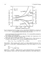
... model for drain-induced barrierlowering and drain-induced high electric field in a short-channel MOSFET , Solid-State pp. 11 8-1 27 (1989). Electron., 30, pp. 50 3-3 11 (1987). [78] Y. Omura and ... (a) and (b) (Figs. 5.31 and 5.32) which are for Vsb = 3 V and 0 V, respectively. n-Channel Devices (nMOST). For n-channel enhancement devices (n' polysil...
Ngày tải lên: 13/08/2014, 05:22