automatic gain control circuit design
Tài liệu Giáo trình kỹ thuật điện: Mạch tự động điều chỉnh độ lợi AGC AUTOMATIC GAIN CONTROL pptx
... và (R - Y) như sau: Giáo trình kỹ thuật điện Mạch tự động điều chỉnh độ lợi AGC AUTOMATIC GAIN CONTROL Ta dùng 2 Transistor T 1 và T 2 dẫn điện ở 2 thời ... cực yếu và đổi lại khi C yếu thì AGC cho phép phân cực mạnh. Với màu AGC có tên là ACC (Automatic Color Control) . hình Khi qua nhiều mạch, sóng tải phụ đổi pha nên sắc của màu bị sai, ta sửa ... giống như trường hợp hệ NTSC 3. Việc thứ ba: xử lý triệt sai pha cho sóng màu: (PHASE CONPENSATOR CIRCUIT) Mạch gồm 3 mạch gọi là bổ chính 3 D hình Delayline của hàng (n + 1) là hàng n Delay...
Ngày tải lên: 15/12/2013, 16:15

Fundamentals of RF Circuit Design With Low Noise Oscillators
... of RF Circuit Design with Low Noise Oscillators. Jeremy Everard Copyright © 2001 John Wiley & Sons Ltd ISBNs: 0-471-49793-2 (Hardback); 0-470-84175-3 (Electronic) 14 Fundamentals of RF Circuit ... 100Ω for a typical 1mA device. The 3dB point for h 21 (short circuit current gain) when placed directly in a common emitter circuit is: hfe f f T = β (1.22) Therefore f β = 50MHz CR h fhf fe feT π β 2 . == (1.21) Note ... Ω≈ 10 ' bb r for a typical 10mA device. The 3dB point for h 21 (short circuit current gain) when placed directly in a common emitter circuit is f β = f T /h fe . Therefore f β = 50MHz. As: CR f = 1 2 π β (1.24) then...
Ngày tải lên: 08/04/2013, 10:50
Allen and Holberg - CMOS Analog Circuit Design
... E 2 max Allen and Holberg - CMOS Analog Circuit Design Page II.0-3 OBJECTIVE • Provide an understanding of CMOS technology sufficient to enhance circuit design. • Characterize passive components ... Holberg - CMOS Analog Circuit Design II.5-6 IMPROVED LAYOUT METHODS FOR CAPACITORS Corner clipping: Clip corners Street-effect compensation: Allen and Holberg - CMOS Analog Circuit Design Page II.1-6 Etching Etching ... (enhancement) Allen and Holberg - CMOS Analog Circuit Design Page I.2-1 I.1 - INTRODUCTION GLOBAL OBJECTIVES • Teach the analysis, modeling, simulation, and design of analog circuits implemented in CMOS technology. •...
Ngày tải lên: 18/10/2013, 12:15
Tài liệu PRINCIPLES OF ASYNCHRONOUS CIRCUIT DESIGN – A Systems Perspective pdf
... comprises the following groups: Industrial designers with a background in conventional (clocked) digital design who wish to gain an understanding of asynchronous design in order, for example, to establish ... components. If this equivalent circuit model is speed-independent, then the circuit is delay-insensitive. Unfortunately the class of delay-insensitive circuits is rather small. Only circuits composed of ... and arithmetic circuits to provide robust completion indication, and 4-phase bundled-data with SI control at the top levels of design, i.e. some- what different from the Amulet designs. This emphasizes...
Ngày tải lên: 09/12/2013, 21:15

Tài liệu Circuit design with VHDL ppt
... 159 8.1 Introduction 159 8.2 Design Style #1 160 8.3 Design Style #2 (Stored Output) 168 viii Contents TLFeBOOK circuit, and of an ARCHITECTURE, which describes how the circuit should func- tion. ... expected. 1.5 Design Examples As mentioned in the preface, the book is indeed a design- oriented approach to the task of teaching VHDL. The integration between VHDL and Digital Design is achieved ... 1 TLFeBOOK I CIRCUIT DESIGN TLFeBOOK ter, while sequential code is treated in another; data types are discussed in one chap- ter, while operators and attributes are in another; what is at the circuit...
Ngày tải lên: 12/12/2013, 11:16


Digital control systems design identification and implementation
Ngày tải lên: 01/01/2014, 20:28

(Ebook electronics) the Rf and microwave circuit design cookbook (maas, 1998 artech h)
Ngày tải lên: 09/01/2014, 02:00

Ebook Bipolar and MOS analog integrated circuit design 2003 grebene
Ngày tải lên: 09/01/2014, 02:12
Ebook - Radio frequency integrated circuit design
... simple circuits to minimize circuit area, but also low power dissipation to maximize battery life. 1.2 Lower Frequency Analog Design and Microwave Design Versus Radio Frequency Integrated Circuit Design RFIC ... xix 1 Introduction to Communications Circuits 1 1.1 Introduction 1 1.2 Lower Frequency Analog Design and Microwave Design Versus Radio Frequency Integrated Circuit Design 2 1.2.1 Impedance Levels ... Frequency Integrated Circuit Design
Ngày tải lên: 09/01/2014, 02:17

Linear circuit design handbook 2nd edition
... R 3 IN R 1 R 2 IN R 1 R 2 Signal gain ϭ 1 ϩ R 2 /R 1 Noise gain ϭ 1 ϩ R 2 /R 1 Signal gain ϭ ϪR 2 /R 1 Noise gain ϭ 1 ϩ R 2 /R 1 Signal gain ϭ ϪR 2 /R 1 Noise gain ϭ 1 ϩ • Voltage noise and ... reflected to the output by the noise gain. • Noise gain, not signal gain, is relevant in assessing stability. • Circuit C has unchanged signal gain, but higher noise gain, thus better stability, ... be less than unity for the inverting case. Signal gain is the gain that we are primarily interested in when designing circuits. The signal gain for an inverting amplifi er stage is: A R R FB IN ϭϪ ...
Ngày tải lên: 09/01/2014, 16:59

Tài liệu Rf Mems Circuit Design For Wireless Communications pptx
... − +××× 44 4 24 4 1 3 3 p (2.29) 28 RF MEMS Circuit Design for Wireless Communications 2 Elements of RF Circuit Design 2.1 Introduction The design of RF MEMS circuits for wireless applications is predicated ... thin-film microstrip lines and equivalent distributed circuit model. RF MEMS Circuit Design for Wireless Communications Wireless SystemsA Circuits Perspective 13 Transceiver and Baseband Phase ... familiar with the fundamentals of both RF MEMS and traditional RF and microwave circuit design. Chapter 1 of RF MEMS Circuit Design for Wireless Communications starts by clearly stating the ubiquitous...
Ngày tải lên: 19/01/2014, 20:20
Tài liệu Analog Integrated Circuit Design P1 docx
... Mirrors 137 Cascode Gain Stage 140 MOS Differential Pair and Gain Stage 142 Bipolar Current Mirrors 146 Bipolar Gain Stages 1 49 16 Chapter 1 lntegratedCircuitDevicesandModelling ... connected to the most negativc voltage in a microcircuit. Ln analog circuits, this might be the negative power supply. but in digital circuits it is normally ground or 0 V. This connection ... Integrated -Circuit Devices and Modelling In this chapter, the operation and modelling of semiconductor devices are described. Although it is possible to do simple integrated -circuit design with...
Ngày tải lên: 26/01/2014, 01:20
Tài liệu Analog Integrated Circuit Design P2 docx
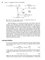
... calculate the gain g,rds = 52.6, which is the largest voltage gain this single transistor can achieve for these operating bias conditions. As we will see, this gain of 52.6 is ... used in circuits with large voltage gain. Cgd is primarily due to the overlap between the gate and the drain and fringing capacitance. Its value is given by where, once again, Lo, ... gate-source voltage. In most circuit applications, noncutoff MOS- FET transistors are operated in strong inversion, with Veff > 100 mV (many prudent circuit designers use a minimum...
Ngày tải lên: 26/01/2014, 01:20

Tài liệu carbon nanotube synthesis device fabrication and circuit design pdf
Ngày tải lên: 23/02/2014, 02:20


Process Variations and Probabilistic Integrated Circuit Design pot
... not only in the design of analog circuits as already done, but also in the digital design process. The great challenge is to assure the functionality of high complex digital circuits with respect ... conditions and does provide the circuit developer with certain design information. For example, the designer can determine whether the leakage current of a given cell or circuit is greater than a key threshold ... Digital Controlled Potentiometer DF Distribution function DFM Design for manufacturability DFY Design for yield DIBL Drain-induced barrier lowering DNL Differential Nonlinearity DoE Design of...
Ngày tải lên: 07/03/2014, 08:20