0
  1. Trang chủ >
  2. Kỹ Thuật - Công Nghệ >
  3. Kĩ thuật Viễn thông >

MOSFET MODELING FOR VLSI SIMULATION - Theory and Practice Episode 8 potx

MOSFET MODELING FOR VLSI SIMULATION - Theory and Practice Episode 8 potx

MOSFET MODELING FOR VLSI SIMULATION - Theory and Practice Episode 8 potx

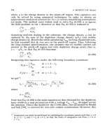
... Qb = - cuxY = - cuxY (6 .88 ) Further, since Qi << Qb, we have Q, z Qb, so that Eq. (6.19) becomes Qb Vgb = Vfb + 4ss - CUX Solving Eqs. (6 .88 ) and (6 .89 ) for 4,s ... form that at first glance appears different. 6.7 Short-Geometry Models 3 - 2- - a 9- W- (7 5 9 1.75 Q t- 6 !I 3 t- 6 fJY 0.5 293 I = 1.31 x 10⁴V/cm a= 1.13 0 - ... &eff as (6.1 48) where 5 = 0.5 for n-channel devices, and 5 = 0.25 - 0.30 for p-channel devices." Using Qb from Eq. (6. 78) and Qi from Eq. (6.79) in Eq. (6.1 48) we get In...
  • 40
  • 255
  • 0
MOSFET MODELING FOR VLSI SIMULATION - Theory and Practice Episode 1 potx

MOSFET MODELING FOR VLSI SIMULATION - Theory and Practice Episode 1 potx

... case permission to photocopy is not required from the publisher. ISBN-13 97 8- 9 8 1-2 5 6 -8 6 2-5 ISBN- 10 98 1 -2 5 6 -8 62-X Disclaimer: This book was prepared by the authors. Neither the Publisher ... Simulation, Kluwer Academic Publisher, Boston, 1 988 . S. Selberherr, Analysis and Simulation of Semiconductor Devices, Springer-Verlag, Wien, New-York, 1 984 . pp. 7 0 -8 0, July 1 987 . ... Qassemzadeh, and T. R. Scott, ‘Algorithms for ASTAP-A network-analysis program’, IEEE Trans. on Circuit Theory, CT-20,pp. 62 8- 6 34 (1973). Also see, Program Reference Manual, Pub. no. SH2 0-1 11 8- 0 ,...
  • 40
  • 270
  • 0
MOSFET MODELING FOR VLSI SIMULATION - Theory and Practice Episode 9 potx

MOSFET MODELING FOR VLSI SIMULATION - Theory and Practice Episode 9 potx

... section 6 .8. 3 08 3 .O 6 MOSFET DC Model I I 1 I I I pMOST toX = 105 A W,/L, = 10l0.5 v,, = -4 v h c E 4 v U I 1 .o I - -2 v 0.01 -1 - - 7- -1 - - i - I * ... Divekar and R. I. Dowell, ‘A depletion-mode MOSFET model for circuit simulation , IEEE Trans. Computer-Aided Design, CAD-3, pp. 8 0 -8 7 (1 984 ). [43] D. Ma, ‘A physical and SPICE-compatible ... ED-34, pp. 8 9-9 3 (1 987 ). [60] J. W. Watt and J. D. Plummer, ‘Universal mobility-field curves for electrons and holes in MOS inversion layers’, Proc. Symp. VLSI Tech., pp. 8 1 -8 2 (1 987 )....
  • 40
  • 269
  • 0
MOSFET MODELING FOR VLSI SIMULATION - Theory and Practice Episode 14 potx

MOSFET MODELING FOR VLSI SIMULATION - Theory and Practice Episode 14 potx

... Therefore, if (P - Pt)’C- ’(P - PJ = P 2 (10.64) 10.6 Parameter Extraction Using Optimizer 53 1 lo-' 1 0-2 1 0-3 9 lo4 I 0-5 1 0-6 1 lo-' 1 0-2 1 0-3 9 lo4 I 0-5 ... Solid-state Electron., Vol. 18, pp. 16 1-1 68 (1975). [ 38] N. D. Arora and M. Sharma, MOSFET substrate current model for circuit simulation , IEEE Trans. Electron Devices, Vol. ED- 38, pp. ... Nagchoudhuri, and S. C. Rustagi, ‘On-line extrac- tion of model parameters of a long buried-channel MOSFET , IEEE Trans. Electron Devices, ED-32, pp. 54 5-5 50 (1 983 ). [4] D. E. Ward and K. Doganis,...
  • 40
  • 394
  • 0
MOSFET MODELING FOR VLSI SIMULATION - Theory and Practice Episode 2 ppt

MOSFET MODELING FOR VLSI SIMULATION - Theory and Practice Episode 2 ppt

... conditions is given by the Fermi-Dirac At 77K ni for silicon is -1 0-2 0cm-3, while at 400K its value is -1 O'*~m-~ 28 2 Basic Semiconductor and pn Junction Theory nonequilibrium condition ... 1 982 and given in many textbooks) by as much as 50% for boron doped p-type silicon. For phosphorous doped n-type silicon the difference is only 1574. Curves for n-type are lower than p-doped ... - Vd); vd is positive for forward bias and negative for reuerse bias. If the applied forward voltage is exactly equal to the built-in voltage, there will be no barrier and therefore,...
  • 40
  • 368
  • 0
MOSFET MODELING FOR VLSI SIMULATION - Theory and Practice Episode 3 docx

MOSFET MODELING FOR VLSI SIMULATION - Theory and Practice Episode 3 docx

... + + pMOST - - - + terminal voltages as drain-source voltage Vds( = V, - VJ, gate-source voltage V,,( = V, - V,), and bulk-source voltage vb,( = vb - Vs). For normal DC ... heavily doped p+ source and drain regions with 80 Z 4 LL 0 - W/L = to, = V. 3 MOS Transistor Structure and Operation -4 .0 -3 .2 -2 .4 -1 .6 -0 .8 0 0 .8 1.6 GATE VOLTAGE, VgS ... Semiconductor and pn Junction Theory The variables F,,F, and F3 are F, =- *bi [l -( 1 - F,)&apos ;-& quot;] (1 -4 F2 = (1 - F,)l+m F, = 1 - F,(1 + m) (2 .87 ) where F,...
  • 40
  • 306
  • 0
MOSFET MODELING FOR VLSI SIMULATION - Theory and Practice Episode 4 doc

MOSFET MODELING FOR VLSI SIMULATION - Theory and Practice Episode 4 doc

... IEEE-IEDM82, Tech. Dig., p. 6 2- (1 982 ). See also R. D. Rung, ‘Trench isolation prospects for application in CMOS VLSI , IEEE-IEDM84, Tech. Dig., p. 57 4-5 78 (1 984 ). pp. 23 8- 2 41 (1 988 ). ... 60 R Rco 18 78 R R," 17 52 R 0.35 y 0.25 50 50 110 3 MOS Transistor Structure and Operation ~i 1; L 6i! - - - - - - - - - Fig. 3.3 1 Cross-section showing ... order expression for Rsp, based on the assumption of uniform doping 1 28 4 MOS Capacitor I- -t > O O+ -0 .6 1 A1 (p-Si n+ Po~y(p-si) -o -8 -I .o Nb (~rn-~) _t Fig. 4.5...
  • 40
  • 292
  • 0
MOSFET MODELING FOR VLSI SIMULATION - Theory and Practice Episode 5 ppsx

MOSFET MODELING FOR VLSI SIMULATION - Theory and Practice Episode 5 ppsx

... df Qh Y <h VTO nMOST p-type - +- +++ pMOST n-type - -+ - (for metals and n+ polysilicon gate) - - (for metals and n+ polysilicon gate) + (for p+ polysilicon gate) (tax ... simulation of MOS capacitance’, IEEE Trans. Computer-Aided Design, CAD-2, pp. 11 1-1 16 (1 983 ). 23 8- 2 41 (1 988 ). 153 9- 1544 (1990). 26, pp. 36 1-3 64 (1 983 ). ... ED-27, pp. 91 4-9 20 (1 980 ). [27] R. R. Troutman, ‘Ion-implanted threshold voltage tailoring for insulated gate field- effect transistors’, IEEE Trans. Electron Devices, ED-24, pp. 18 2-1 92...
  • 40
  • 224
  • 0
MOSFET MODELING FOR VLSI SIMULATION - Theory and Practice Episode 6 pptx

MOSFET MODELING FOR VLSI SIMULATION - Theory and Practice Episode 6 pptx

... >" ;- I 5 0.4 lY I bO.3 195 1'1'1'1'1~1'1'1~ I - Nb = 2 X 10'"cm-3 - - - - - W=20 m - f"\L "A&ING - I I 1 ... (a) - - - 16 -3 A Nb=1.71 x 10 cm x Nb = 1.5 6 x 1Ol6c m3 N 4-2 5 x 1 0'6cm-3 0. 3- 2 6 10 I& I8 2 WIDTH (pm) (b) Fig. 5.21 (a) Aker's model for ... 5.2 Nonuniformly Doped MOSFET i 185 f (a) (b) Fig. 5.10 (a) Step doping profile for an n-channel MOSFET, (b) Doping transformation pro- cedure for calculating the equivalent...
  • 40
  • 218
  • 0
MOSFET MODELING FOR VLSI SIMULATION - Theory and Practice Episode 7 doc

MOSFET MODELING FOR VLSI SIMULATION - Theory and Practice Episode 7 doc

... field in a short-channel MOSFET , Solid-State pp. 11 8- 1 27 (1 989 ). Electron., 30, pp. 50 3-3 11 (1 987 ). [ 78] Y. Omura and K. Ohwada, ‘Threshold voltage theory for short-channel MOSFET model ... pp. 38 4-3 87 (1 981 ). [67] L. A. Akers, M. Sugino, and J. M. Ford, ‘Characterization of the inverse-narrow-width effect’, IEEE Trans. Electron Devices, ED-34, pp. 247 6-2 484 (1 987 ). [ 68] K. ... geometry MOSFET , Solid-state Electron., 26, pp. 85 1 -8 60(1 983 ). [76] S. C. Chamberlain and S Ramanan, ‘Drain-induced barrier-lowering analysis in VLSI MOSFET devices using two-dimensional...
  • 40
  • 294
  • 0

Xem thêm

Từ khóa: Báo cáo thực tập tại nhà thuốc tại Thành phố Hồ Chí Minh năm 2018Nghiên cứu tổ chức pha chế, đánh giá chất lượng thuốc tiêm truyền trong điều kiện dã ngoạiMột số giải pháp nâng cao chất lượng streaming thích ứng video trên nền giao thức HTTPNghiên cứu tổ chức chạy tàu hàng cố định theo thời gian trên đường sắt việt namGiáo án Sinh học 11 bài 13: Thực hành phát hiện diệp lục và carôtenôitGiáo án Sinh học 11 bài 13: Thực hành phát hiện diệp lục và carôtenôitĐỒ ÁN NGHIÊN CỨU CÔNG NGHỆ KẾT NỐI VÔ TUYẾN CỰ LY XA, CÔNG SUẤT THẤP LPWANNGHIÊN CỨU CÔNG NGHỆ KẾT NỐI VÔ TUYẾN CỰ LY XA, CÔNG SUẤT THẤP LPWAN SLIDEQuản lý hoạt động học tập của học sinh theo hướng phát triển kỹ năng học tập hợp tác tại các trường phổ thông dân tộc bán trú huyện ba chẽ, tỉnh quảng ninhPhối hợp giữa phòng văn hóa và thông tin với phòng giáo dục và đào tạo trong việc tuyên truyền, giáo dục, vận động xây dựng nông thôn mới huyện thanh thủy, tỉnh phú thọTrả hồ sơ điều tra bổ sung đối với các tội xâm phạm sở hữu có tính chất chiếm đoạt theo pháp luật Tố tụng hình sự Việt Nam từ thực tiễn thành phố Hồ Chí Minh (Luận văn thạc sĩ)Phát triển du lịch bền vững trên cơ sở bảo vệ môi trường tự nhiên vịnh hạ longNghiên cứu tổng hợp các oxit hỗn hợp kích thƣớc nanomet ce 0 75 zr0 25o2 , ce 0 5 zr0 5o2 và khảo sát hoạt tính quang xúc tác của chúngTìm hiểu công cụ đánh giá hệ thống đảm bảo an toàn hệ thống thông tinThiết kế và chế tạo mô hình biến tần (inverter) cho máy điều hòa không khíTăng trưởng tín dụng hộ sản xuất nông nghiệp tại Ngân hàng Nông nghiệp và Phát triển nông thôn Việt Nam chi nhánh tỉnh Bắc Giang (Luận văn thạc sĩ)Tranh tụng tại phiên tòa hình sự sơ thẩm theo pháp luật tố tụng hình sự Việt Nam từ thực tiễn xét xử của các Tòa án quân sự Quân khu (Luận văn thạc sĩ)Giáo án Sinh học 11 bài 14: Thực hành phát hiện hô hấp ở thực vậtChiến lược marketing tại ngân hàng Agribank chi nhánh Sài Gòn từ 2013-2015MÔN TRUYỀN THÔNG MARKETING TÍCH HỢP