scanning electron microscopy and nanotechnology
Báo cáo hóa học: " Memory properties and charge effect study in Si nanocrystals by scanning capacitance microscopy and spectroscopy" docx
... to be injected and trapped than electrons In this letter, Si-ncs were formed on top of a thermally grown silicon dioxide layer SCM and SCS were used to study the memory properties and charge effect ... by SCM/SCS at the nanometer scale Page of 12 Kopanski JJ, Marchiando JF, Lowney JR: Scanning capacitance microscopy measurements and modeling: Progress towards dopant profiling of silicon J Vac ... doi:10.1186/1556-276X-6-163 Cite this article as: Lin et al.: Memory properties and charge effect study in Si nanocrystals by scanning capacitance microscopy and spectroscopy Nanoscale Research Letters 2011 6:163 Acknowledgements...
Ngày tải lên: 21/06/2014, 05:20

Studies of self assembled monolayers on highly oriented pyrolytic graphite using scanning tunneling microscopy and computational simulation 1
... nano-devices development, and biological process Works of thiols adsorbed on gold surfaces by Nuzzo and Allara [13, 15] in the early 1980s and trichlorosilanes on silicon oxide by Maoz and Sagiv [13, 16] ... conductivity, flatness, and inertness provide us a suitable environment for STM experiments Last but not least, the structure of the HOPG is well understood and relatively simple and any possible interactions ... top layer: the ‘white’ carbon atoms and the ‘black’ carbon atoms The ‘black’ carbon atoms exhibit a higher local electronic density of states near Fermi level and are therefore expected to appear...
Ngày tải lên: 14/09/2015, 08:37

Studies of self assembled monolayers on highly oriented pyrolytic graphite using scanning tunneling microscopy and computational simulation 2
... References [1] Wiesendanger, R Scanning Probe Microscopy and Spectroscopy Methods and applications, Cambridge University Press, 1994 [2] Bai, C.L., Scanning tunneling microscopy and its application, Scientific ... the diversity of STM and STM-based technological applications: STM can achieve lateral and vertical resolutions of 0.1nm and 0.01nm, respectively, i.e., individual atoms and molecules can be ... the Scanning Tunneling Microscope (STM) was introduced, it still remained a dream to directly observe geometric and electronic surface structures at the atomic level at ambient pressure and room...
Ngày tải lên: 14/09/2015, 08:37
Studies of self assembled monolayers on highly oriented pyrolytic graphite using scanning tunneling microscopy and computational simulation 3
... production and detection of sound, generation of high voltages, electronic frequency generation, microbalance, and ultra fine focusing of optical assemblies It is also the basis of operation of the scanning ... the basis of operation of the scanning probe microscope, such as STM and AFM Scanner serve as the “movers and shakers” of every scanning probe microscope 39 CALIBRATION Typically, they consist of ... of sizes and angles The user then specifies the distance between known features on the reference’s surface and a parameter is recorded to compensate the scanner’s movements The X, Y and Z axes...
Ngày tải lên: 14/09/2015, 08:37

Studies of self assembled monolayers on highly oriented pyrolytic graphite using scanning tunneling microscopy and computational simulation 4
... Proposed adsorption site and orientation of first adsorbed alkyl group on HOPG surface (top view): The dark lines on the left hand side and middle of the picture are step and adsorbate respectively ... Model A and B with graphite lattice being set to invisible Two models A and B are shown in Fig 4.9 Model A consisted of two levels of graphite (0 1) sheet with each containing 12×30 cells and an ... energy of the whole cluster Apparently, Models A and B have the same E(surface) and E(adsorbate) since they have the same HOPG surface lattice and the same number of adsorbates The E(adsorbate/surface)...
Ngày tải lên: 14/09/2015, 08:37

Studies of self assembled monolayers on highly oriented pyrolytic graphite using scanning tunneling microscopy and computational simulation 5
... there are two major sections A and B within the area scanned (60nm×60nm) The DDPER lamella has a 33° angle and 77° angle with horizontal direction within section A and B, respectively, as indicated ... can be carried out subsequently The distance between the oxygen and surface increased to 3.3nm and 3.5nm for Cluster A (DDPER/HOPG) and Cluster B (S170/HOPG) respectively after geometry optimization ... effect can be varied correspondingly The chemical structures of the DDPER and its four derivatives (S170, S169, S171, and S172) are shown below: O C12H25 N O C12H25 N O O Br O N O C12H25 O DDPER...
Ngày tải lên: 14/09/2015, 08:37
Studies of self assembled monolayers on highly oriented pyrolytic graphite using scanning tunneling microscopy and computational simulation 6
... changes and the symmetry breaking which results in chirality [9, 12, 17, 21-25] The development of the scanning probe techniques especially scanning tunneling microscopy (STM) and atomic force microscopy ... showed that the unit cell on the right hand side is rectangular with two sides at a=4.000.08nm and b=2.950.06nm On the contrary, the unit cell on the left hand side is rhombic with two sides at ... the HHB and graphite surface, although no covalent bonds were formed The resulting products or the physisorbed molecules were shown in and when graphite attacked HHB through route (L-HHB) and (R-HHB),...
Ngày tải lên: 14/09/2015, 08:37

Studies of self assembled monolayers on highly oriented pyrolytic graphite using scanning tunneling microscopy and computational simulation 7
... monolayers, the use of scanning tunneling microscopy and the scanning results had been discussed in detail in reviews by De Feyter [3, 4], Wan [5] and Tao [6] But Matzger and his coworkers’ attempt ... left hand side As [SP] decreases equilibrium (7-3) will also shift to the left hand side, and cause the melting of the SAMs 7.5 Common properties of 3D crystals and 2D crystals 3D crystals and ... dipole-dipole interaction, and etc 7.4.4.1 Molecular Structures and Symmetry Linear organic molecules including saturated and unsaturated n-alkanes, n-alkyl acids, and n-alcohols exhibit good...
Ngày tải lên: 14/09/2015, 08:37

Scanning Microscopy for Nanotechnology Techniques and Applications pdf
... Scanning Microscopy for Nanotechnology Scanning Microscopy for Nanotechnology Techniques and Applications edited by Weilie Zhou University of New Orleans New Orleans, Louisiana and Zhong ... for secondary and BSEs; energy-dispersive x-ray spectrometer and Fundamentals of Scanning Electron Microscopy 23 Scanning coils Scanning signal generator Final aperture Backscattered electron detector ... transmitted electrons can be used to acquisition of elemental information and distribution The integration of scanning electron beam with a transmission electron microscopy detector generates scanning...
Ngày tải lên: 27/06/2014, 10:20
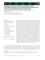
Báo cáo khoa học: Structure of the atrial natriuretic peptide receptor extracellular domain in the unbound and hormone-bound states by single-particle electron microscopy ppt
... mechanism Fig Single-particle EM of apoECD and ANP–ECD (A) Representative electron micrograph and (B) class averages obtained for apoECD Similar electron micrographs and class averages were obtained for ... conditions and in the absence of crystal contacts In this study, we have carried out single-particle image reconstruction of the ECD dimer with and without bound ANP using electron microscopy ... single-particle EM and Trp fluorescence studies for the transmembrane signaling mechanism of the ANP receptor are discussed Results and Discussion EM and single-particle reconstruction From electron micrographs...
Ngày tải lên: 07/03/2014, 03:20

electron microscopy methods and protocols
... A W and Wilson, A J (1993) Basic Biological Preparation Techniques for TEM, in Procedures in Electron Microscopy, Wiley, England, ch 5 Newman, G R and Hobot, J A (1993) Resin Microscopy and On-Section ... method for high resolution electron microscopy of viruses Biochim Biophys Acta 34, 60–71 Harris, J R (1997) Negative staining and cryoelectron microscopy, RMS Microscopy Handbook, Number 35, BIOS ... the subtleties and hazards of this oversimplified description will be expanded upon below, and have recently From: Methods in Molecular Biology, vol 117: Electron Microscopy Methods and Protocols...
Ngày tải lên: 10/04/2014, 23:20

scanning microscopy for nanotechnology
... for secondary and BSEs; energy-dispersive x-ray spectrometer and Fundamentals of Scanning Electron Microscopy 23 Scanning coils Scanning signal generator Final aperture Backscattered electron detector ... transmitted electrons can be used to acquisition of elemental information and distribution The integration of scanning electron beam with a transmission electron microscopy detector generates scanning ... the electron beam and specimen interactions These interactions can be divided into two major categories: elastic interactions and inelastic interactions 1 Fundamentals of Scanning Electron Microscopy...
Ngày tải lên: 04/06/2014, 14:41

Scanning thermal microscopy methodology for accurate and reliable thermal measurement
... Roadmap for Semiconductor DRAM Dynamic Random Access Memory NA Numerical Aperture MPU Microprocessor SThM Scanning Thermal Microscopy SJEM Scanning Joule Expansion Microscopy PID Proportional-integral-derivative ... convection and radiation In electronic devices, electron flow occurs in metals and semiconductors For heat, it flows through all materials Convection is the main heat transfer mechanism in liquids and ... on scanning probe microscopy have enabled direct observation of various phenomena on nanoscale devices and structures with high spatial resolution One of such techniques, Scanning Thermal Microscopy...
Ngày tải lên: 09/09/2015, 18:57

Application of biased scanning probe microscopy techniques for multifunctional characterization of bifeo3 and zno thin films
... hysteresis loop Forward and reverse coercive voltages, V+ and V−, nucleation voltages Vc+ and Vc− , + − and forward and reverse saturation and remnant responses, R0 , R0 , Rs+ and Rs− , are shown ... potential future materials for advanced electronic applications Scanning probe microscopy techniques, Piezoresponse Force Microscopy (PFM) and Kelvin Probe Force Microscopy (KPFM) are used in this ... amplitude (dzz) and Surface potential results for all the samples under stress and magnetic field at location and Table 6.1 Mean domain angle under the unbiased and biased area for undoped and 2%Mg...
Ngày tải lên: 10/09/2015, 08:41
Nanostructure, biopiezoelectric and bioferroelectric behaviors of mollusk shells studied by scanning probe microscopy techniques
... [(c) and (d)] and DART-LPFM [(e) and (f)] are scanned (500× 500 nm , 256× 256 pixels); (c) and (e) are the amplitude images; (d) and (f) are the phase images Fig 5.6 DART-VPFM [(b) and (c)] and ... [(g) and (i)] and phase [(h) and (j)] images in the lateral direction All of the amplitude images show the piezoresponse at Vac Last row are the magnitude [(k) and (m)] and argument [(l) and (n)] ... 2nd and 3rd column (400× 400 nm ): observed from the interior and boundary of platelet on the nacre surface (a) (d) and (g) are height images, (b) (e) and (h) are amplitude images, and (c) (f) and...
Ngày tải lên: 10/09/2015, 09:23

Dielectric characterization and dopant profile extraction using scanning capacitance microscopy
... SPM Scanning Probe Microscopy (SPM) Scanning Tunnelling Microscopy (STM) 1981-1982 Scanning Ion Conductance Microscopy (SICM) Atomic Force Microscopy (AFM) 1986 Scanning Near Field Optical Microscopy ... (SNOM) Scanning Capacitance Microscopy (SCM) Magnetic Force Microscopy (MFM) Photon Scanning Tunnelling Microscopy (PSTM) Scanning Thermal Microscopy (STHM) Electrostatic Force Microscopy (EFM) Scanning ... Potential Microscopy (SCPM) Shear Force Microscopy (SHFM) Figure 2.1 : The different types of scanning probe microscopy techniques 2.2 Initial Developments of Scanning Capacitance Microscopy...
Ngày tải lên: 14/09/2015, 18:36

Growth and transmission electron microscopy studies of nanomaterials 1 2
... Chemical and electronic structure 1.3.2 Chemical and electronic structure; elemental distribution and phase mapping electric and magnetic fields Observing dynamic phase transformation process and ... holograms using electron waves in TEM The most frequently used techniques for imaging the magnetic domain structures are Fresnel contrast, and Lorentz microscopy and off-axis electron holography ... nanostructure 1.3.4.1 Temperature and electron beam induced phase transformation In situ studies of the temperature and electron beam induced phase transformations and chemical evolution of nanocrystals...
Ngày tải lên: 16/09/2015, 08:30

Growth and transmission electron microscopy studies of nanomaterials 3 4
... before (lower) and after (upper) exposure to NH3, showing the B 1s and N 1s K-edges, and a notable absence of carbon TEM observation of the particles revealed excellent size uniformity, and figure ... liquid and solid defines the wetting behaviour of the liquid, and obeys the classical equation of Young: cos θ = σ SV − σ SL σ LV where σSV, σSL and σLV are the solid: vapour, solid: liquid and ... to its direct and wide-bandgap of 3.72 eV, ZnS has attracted great attention for its technological utility such as manufacture of pigments, phosphorluminescent screens and optoelectronics Currently,...
Ngày tải lên: 16/09/2015, 08:30
Growth and transmission electron microscopy studies of nanomaterials 5 7
... Largest difference map peak and hole, (e.Å-3) 0.791 and -0.799 0.438 and -0.467 6957 / 21 / 392 TG and DTA reveal that the compounds and start decomposing at 80-130 ˚C and the residual weight when ... synthesized and characterized [(Ph3P)2Cu(µ-ER)2M(ER)2] (M = Ga and In; E = S, Se; R = Et and Bui) and [Bu2In(SPr)Cu(S2CNPri2)] have been used to prepare thin films of CuInS2, CuInSe2 and CuGaS2 ... controlled by ligand design Ligand and metal are closely associated Low temperature growth is possible Therefore, in last two decades, chemists have been interested in synthesizing stable and efficient...
Ngày tải lên: 16/09/2015, 08:30
Bạn có muốn tìm thêm với từ khóa: