measurements residual stresses and materials characterization of thin films
The Materials Science of Thin Films 2010 pptx
... The Materials Science of Thin Films I I I The Materials Science of Milton Ohring Stevens Institute of Technology Department of Materials Science and Engineering Hoboken, ... stability, formation, and solid-state reactions in thin films Much of this chapter is a condensed adaptation of standard treatments of bulk materials, but it is equally applicable to thin films Nevertheless, ... understanding of the fundamental nature of materials throughout much of the twentieth century has led to the development of materials science and engineering This period witnessed the emergence of...
Ngày tải lên: 05/03/2014, 17:20
Báo cáo hóa học: " Effect of Composition on Electrical and Optical Properties of Thin Films of Amorphous GaxSe1002x Nanorods" pptx
... well-established knowledge of the electrical and optical properties of GaSe thin films, in this paper, we report the results on electrical and optical measurements of amorphous thin films of GaSe nanorods ... diameter of the nanorods varies from 140 to 180 nm, and the length is of several hundreds of nanometers Figure presents the temperature dependence of the dc conductivity of thin films of a- GaxSe100-x ... frequency doubling and fast optical gating [11] and behaves as an X-ray detector [12] Electronic and optoelectronic properties of GaSe, GaS, and InSe materials indicate the possibilities of realizing...
Ngày tải lên: 21/06/2014, 17:20

The Materials Science of Thin Films potx
... The Materials Science of Thin Films I I I The Materials Science of Milton Ohring Stevens Institute of Technology Department of Materials Science and Engineering Hoboken, ... stability, formation, and solid-state reactions in thin films Much of this chapter is a condensed adaptation of standard treatments of bulk materials, but it is equally applicable to thin films Nevertheless, ... understanding of the fundamental nature of materials throughout much of the twentieth century has led to the development of materials science and engineering This period witnessed the emergence of...
Ngày tải lên: 27/06/2014, 06:20

The Materials Science of Thin Films 2011 pptx
... The Materials Science of Thin Films I I I The Materials Science of Milton Ohring Stevens Institute of Technology Department of Materials Science and Engineering Hoboken, ... stability, formation, and solid-state reactions in thin films Much of this chapter is a condensed adaptation of standard treatments of bulk materials, but it is equally applicable to thin films Nevertheless, ... understanding of the fundamental nature of materials throughout much of the twentieth century has led to the development of materials science and engineering This period witnessed the emergence of...
Ngày tải lên: 27/06/2014, 17:20

The Materials Science of Thin Films 2011 Part 1 ppt
... The Materials Science of Thin Films I I I The Materials Science of Milton Ohring Stevens Institute of Technology Department of Materials Science and Engineering Hoboken, ... stability, formation, and solid-state reactions in thin films Much of this chapter is a condensed adaptation of standard treatments of bulk materials, but it is equally applicable to thin films Nevertheless, ... understanding of the fundamental nature of materials throughout much of the twentieth century has led to the development of materials science and engineering This period witnessed the emergence of...
Ngày tải lên: 11/08/2014, 20:21
The Materials Science of Thin Films 2011 Part 2 ppsx
... Thermodynamics of Materials R A Swalin, Thermodynamics of Solids, Wiley, New York (1962) C H Lupis, Chemical Thermodynamics of Materials, North-Holland, New York (1983) 48 A Review of Materials Science ... Structure and Properties of Materials, Vols 1-4, Wiley, New York (1964) M Ohring, Engineering Materials Science, Academic Press, San Diego (1995) L H Van Vlack, Elements of Materials Science and Engineering, ... purpose Threads of this chapter will be woven into the subsequent fabric of the discussion on the preparation and properties of thin films An FCC film is deposited on the (100) plane of a single-crystal...
Ngày tải lên: 11/08/2014, 20:21
The Materials Science of Thin Films 2011 Part 4 ppt
... resistant A1 films, and epitaxial Si, GaAs, Gap, and InSb films deposited at low temperatures are some examples indicative of the excellent properties of ICB films Among the advantages of ICB deposition ... (1976) 11 L Holland, Vacuum Deposition of Thin Films, Wiley, New York (1956) 12 C H Ting and A R Neureuther, Solid State Technol 25(2), 115 (1982) 13 H L Caswell, in Physics of Thin Films, Vol 1, ... Westwood, in Physics of Thin Films, Vol 14, eds M H Francombe and J L Vossen, Academic Press, New York (1989) 26.* L I Maissel and M H Francombe, An Introduction to Thin Films, Gordon and Breach, New...
Ngày tải lên: 11/08/2014, 20:21
The Materials Science of Thin Films 2011 Part 5 docx
... Coalescence and Depletion 5.5 Experimental Studies of Nucleation and Growth 5.6 Grain Structure of Films and Coatings 5.7 Amorphous Thin Films References 1-5 are recommended sources for much of the ... function of A H c comment on the gas transport direction and magnitude as a function of the sign and value of A H In growing epitaxial Ge films by the disproportionation reaction of Eq Exercises ... or grown by both PVD and CVD methods In a report compare the resultant structures stoichiometries and properties The Journal of Vacuum Science and Technology and Thin Solid Films are good references...
Ngày tải lên: 11/08/2014, 20:21
The Materials Science of Thin Films 2011 Part 6 doc
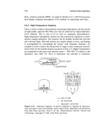
... to monitor the in situ deposition and growth of thin films on well-polished, reflecting substrates, such as Si and GaAs Because of its Characterization of Thin Films 260 \ \ O Al DE LT * e:no ldeg.) ... A to 65 pm, and the vertical resolution is 10 A - 262 Characterization of Thin Films One of the important applications of stylus measurements is to determine the flatness and depth of a sputtered ... seeing is believing and understanding, the SEM is perhaps the most widely employed thin- film and coating characterization instrument A schematic 266 Characterization of Thin Films of the typical SEM...
Ngày tải lên: 11/08/2014, 20:21

The Materials Science of Thin Films 2011 Part 8 pps
... alternately on for 0.5 and off for during the entire run Film thickness measurements showed that 1.80 pm of GaAs and 0.35 pm of AlAs were deposited a b c d What are the growth rates of GaAs and Al,G, -,As? ... high modulus of elasticity and high hardness enable Si wafers to withstand the rigors of handling and device processing Its great natural abundance, the ability to readily purify it and the fact ... Fundamentals of Diffusion films Aspects of both of these broad applications will be discussed in this chapter in a fundamental way within the context of the following subjects: 8.2 Fundamentals of Diffusion...
Ngày tải lên: 11/08/2014, 20:21
The Materials Science of Thin Films 2011 Part 9 pot
... application of external loading and are said to possess internal or residual stresses The origin and nature of these internal residual stresses are the sources of many mechanical effects in films and ... in the handling of thin films has posed a great experimental challenge and stimulus to the ingenuity of investigators Detachment of films from substrates and methods for gripping and aligning them, ... S Ho, and K N Tu, eds., Low Temperature Diffusion and Applications to Thin Films, Elsevier, Lausanne (1975); also Thin Solid Films 25 (1975) J M Poate, K N Tu, and J W Mayer, eds., Thin Films- Znterdiffusion...
Ngày tải lên: 11/08/2014, 20:21

The Materials Science of Thin Films 2011 Part 10 pps
... band diagrams and concepts This chapter focuses primarily on the electrical conduction properties of thin metal, insulating, and superconducting films Almost half of the classic Handbook of Thin ... studies on the resistivity of thin metal films from which useful values of p o & (or pf and P ) may be deduced” (Ref 462 Electrical and Magnetic Properties of Thin Films 9) Among the reasons ... on Ta Indium-tin oxide (ITO) films have the 464 Electrical and Magnetic Properties of Thin Films Table 10-1 Electrical Properties of Thin- and Thick-Film Resistor Materials Material Pd-Ag Ni(80)Cr(20)...
Ngày tải lên: 11/08/2014, 20:21

The Materials Science of Thin Films 2011 Part 11 pot
... properties and applications of metal and dielectric thin films 11.2 PROPERTIES OPTICAL OF FILM MATERIALS 11.2.1 General Considerations In order to understand the optical behavior of films and film ... 38 Electrical and Magnetic Properties of Thin Films M H Francombe and R W Hoffman, Academic Press, New York (1975) J G Simmons, in Handbook of Thin Film Technology, eds L I Maissel and R Glang, ... optical films are the magnitudes of n and k, the spectral range of transmission, the dependence of properties on film structure and deposition 518 Optical Propertiesof Thin Films processes, and environmental...
Ngày tải lên: 11/08/2014, 20:21

The Materials Science of Thin Films 2011 Part 12 pptx
... applications of thin films and film systems in optics (From usually with the use of many film layers (sometimes a dozen or more) but with only a very limited number of materials (e.g., MgF, and ZnS) ... increases with number of layers The spectral width of the high reflectance zone is a function of the ratio of the refractive indices of the involved films, and there are a couple of practical ways ... examples Narrow bandpass or monochromatic filters Thin film coatings to achieve these ends consist of thin metal films, dielectric films, multilayer metal and dielectric film combinations, and all dielectric...
Ngày tải lên: 11/08/2014, 20:21

The Materials Science of Thin Films 2011 Part 13 ppt
... Stecura, Thin Solid F l s 136, 241 (1986) 27 R A Miller and C C Berndt, Thin Solid Films 119, 195 (1984) 28 G Johner and K K Schweitzer, Thin Solid Films 119, 301 (1984) Modification of Surfaces and ... Holleck and H Schulz, Thin Solid Films 153, 11 (1987) 11 A Layyous and R Wertheim, J de Phys Colloque C5, 423 (1989) 12 W D Sproul, Thin Solid Films 107, 141 (1983) 13 C A Brookes, Science of Hard Materials, ... 23 H J Boving and H E Hintermann, Thin Solid Films 153, 253 (1987) 24 H E Hintermann, Thin Solid Films 84, 215 (1981) 25 S Mrowec and T Werber, Gas Corrosion of Metals U.S Dept of Commerce, NTIS...
Ngày tải lên: 11/08/2014, 20:21

The Materials Science of Thin Films 2011 Part 14 doc
... processing and the ability to characterize structure-property relationships Thus the spirit of materials science of thin films- the theme and title of this book-is preserved in microcosm within this ... deposition and processing of films, lithographic patterning of small features, and compatibility with other materials and device structures have served to hinder rapid development of microelectronic ... technology The needs of both professional and consumer audio, video, and computer tapes and disks are currently met by an assortment of magnetic particle and thin- film materials However, the insatiable...
Ngày tải lên: 11/08/2014, 20:21

The Materials Science of Thin Films 2011 Part 15 ppt
... Surfaces and Interfaces of Ceramic Materials, eds L C Dufour, C Monty, and G P Ervas, Kluwer Academic, Dordrecht ( 1989) *Recommended texts or reviews 682 Emerging Thin- Film Materials and Appllcatlons ... Microelectronic Materials and Processes, ed R A Levy, Kluwer Academic, Dordrecht (1989) 4.* I Brodie and J A Muray, The Physics of Microfabrication, Plenum Press, New York (1982) J B Angell, S C Terry, and ... simply modeled by an infinite well potential The effective masses of conduction-band electrons and valence-band holes are 0.06moand 0.42m0, respectively a In order to tune operation to 1.0-eV radiation,...
Ngày tải lên: 11/08/2014, 20:21

The Materials Science of Thin Films Episode 7 pps
... combination of M,, M , and 8, the simple formula E, = KwEo (6-22) 290 Characterizationof Thin Films x = 900 A x=o I I b YIELD x=9ooA x=o Figure 6-21 (a) Geoyetry of scattering and notation of energies ... separated and phosphorous doping profiles obtained as shown in Fig 6-26 Characterization of Thin Films 300 Figure 6-26 SIMS depth profile of P implanted in Si obtained with Cs+ ions (Courtesy of H ... This is certainly true of epitaxial films exhibiting island and S.K.growth and most of the films reported in the older literature However, some of today’s lattice-matched MBE films, grown under exacting...
Ngày tải lên: 13/08/2014, 17:20
Design, fabrication and characterization of thin film materials for heterojunction silicon wafer solar cells
... silicon thin films generally have different bandgaps and Fermi levels compared to their crystalline counterpart, the conduction / valence band offsets of the doped and intrinsic silicon thin films ... reported bandgap of amorphous silicon (~1.7 eV) against that of crystalline silicon (1.1 eV), it follows that there is a larger band offset (~0.45 eV) at the valence band edges and a smaller band offset ... properties of the c-Si wafer and of the a-Si and µc-Si thin- film layers, based on [127] as well as on the fitting of the lifetime samples of Figure 4.4 The activation energy (i.e position of the...
Ngày tải lên: 09/09/2015, 11:15