interferometric thin film optical biosensors
báo cáo hóa học:" Structural and optical properties of a radio frequency magnetron-sputtered ZnO thin film with different growth angles" pdf
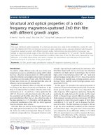
... electrodeposited ZnO thin films Thin Solid Films 2008, 516:3893-3898 Bragg WL, Bragg WH: The Crystalline State New York: McMillan; 1933 15 30 o Growth angle ( ) Figure Reflectance of ZnO films vs growth ... structured ZnO films The ZnO films were deposited on glass substrates inside a specially designed RF magnetron sputtering system We studied the growth angle effect of the films for optical properties ... films All ZnO films showed different patterns according to the wavelength of incidence rays The ZnO film with a 0° growth angle has the lowest reflectance of 10.81% at 418 nm The 15° angled film...
Ngày tải lên: 21/06/2014, 17:20
Tài liệu Báo cáo " Survey of WO3 thin film structure built on ito/glass substrates by the Raman and xrd spectroscopies" doc
... LeGore, R.J Lad, Thin solid films 400 (2001) 56 Huiyao Wang, Pei Xu, Tianmin Wang, Thin solid films 388 (2001) 68 Christian Salinga, Hansjörg Weis, Matthias Wuttig, Thin solid films 414 (2002) ... A Siokou, Thin solid films 384 (2001) 298 H.Y Wong, C.W.Ong, R.W.M Kwok, K.W Wong, S.P Wong, W.Y Cheung, Thin solid films 376 (2000) 131 I Porqueras, E Bertran, Thin solid films 377-378 (2000) ... Nishide, Fujio Mizukami, Thin solid films 295 (1995) 212 A Elshafie, H.H Afify, A Abdel-All, phys stat sol (a) 174 (1999) 301 P.S Patil, P.R.Patil, E.A Ennaoui, Thin solid films 370 (2000) 38 M.J...
Ngày tải lên: 13/02/2014, 03:20

Tài liệu MBA/SMA 0204, MBB/SMA 0207, MBE/SMA 0414 - Precision Thin Film Leaded Resistors pptx
... Beyschlag Precision Thin Film Leaded Resistors DESCRIPTION Production is strictly controlled and follows an extensive set of instructions established for reproducibility A homogeneous film of metal ... FORTH AT www.vishay.com/doc?91000 MBA/SMA 0204, MBB/SMA 0207, MBE/SMA 0414 - Precision Precision Thin Film Leaded Resistors Vishay Beyschlag PACKAGING - Axial products BOX TAPING ACC IEC 60286-1 ... FORTH AT www.vishay.com/doc?91000 MBA/SMA 0204, MBB/SMA 0207, MBE/SMA 0414 - Precision Precision Thin Film Leaded Resistors Vishay Beyschlag PACKAGING - Radial products REEL TAPING ACC IEC 60286-2...
Ngày tải lên: 20/02/2014, 10:20
Enhancement-Mode Metal Organic Chemical Vapor Deposition-Grown ZnO Thin-Film Transistors on Glass Substrates Using N2O Plasma Treatment docx
... (nm) Fig (Color online) PL spectra of the as-grown ZnO films before and after N2 O treatment for 665 s 3.4 XRD, PL, and XPS measurements of ZnO films In order to determine the cause of the enhancement-mode ... Phys 98 (2005) 041301 2) X A Zhang, J W Zhang, W F Zhang, D Wang, Z Bi, X M Bian, and X Hou: Thin Solid Films 516 (2008) 3305 3) K Remashan, D K Hwang, S J Park, and J H Jang: IEEE Trans Electron ... N Blanchard: J Appl Phys 102 (2007) 074512 11) P K Shin, Y Aya, T Ikegami, and K Ebihara: Thin Solid Films 516 (2008) 3767 12) J Siddiqui, E Cagin, D Chen, and J D Phillips: Appl Phys Lett 88...
Ngày tải lên: 05/03/2014, 21:20
gas sensing properties of metal - organics derived pt dispersed - tio2 thin film fired in nh3
... of the thin films was about 70 nm The gas sensitivity of the thin film with Ag electrode was almost the same as that with Au electrode However, Au electrode was easily torn from thin film Therefore, ... on the film fired at 4508C The thin film fired at 4508C proved to have the highest gas sensitivity and selectivity to H among reducing gases: H , CO and CH A XRD profile of this thin film indicated ... in the film fired in NH than in 3% H 2rAr This implies that the nitrogen produced by the decomposition of NH diffuses into thin films and forms Ti–N bonds Moreover, the pretreated thin films were...
Ngày tải lên: 19/03/2014, 16:48
highly sensitive thin film nh3 gas sensor operating at room
... composite is too thin, the response will be decreased Such gas-response dependent on the thickness of the composite MWCNTs/SnO2 thin film sensor has not been clear so far It seems that the thin film composite ... embedded by spherical tin oxide nanoparticles Our sensing element is of a thin film type Therefore, the morphology of the composite thin film after the heat treatment at 550 ◦ C in vacuum of 10−2 Torr ... composites with different MWCNTs contents were prepared for the sensitive thin film fabrication The thickness of the sensitive thin films was controlled by varying spin-coating speed The coating layer...
Ngày tải lên: 19/03/2014, 16:48
influence of polymerization temperature on nh3 response of pani tio2 thin film gas sensor
... between the thin film and the adsorbed gas is a dynamical process Thus, when the thin film is exposed to NH3 gas, the adsorption and desorption processes will simultaneously occur, and the thinner ... Woosuck, N Izu, The preparation of polyaniline intercalated MoO3 thin film and its sensitivity to volatile organic compounds, Thin Solid Films 514 (2006) 329–333 N Parvatikar, S Jain, S Khasim, M Revansiddappa, ... PANI/TiO2 thin films prepared at 0, 10 and 20 ◦ C when exposed to NH3 of various concentrations at room temperature Concentration of NH3 (ppm) Fig UV–vis absorption spectra of a PANI thin film prepared...
Ngày tải lên: 20/03/2014, 13:04
modeling of the conduction in a wo3 thin film as ozone sensor
... Perczel, Z Sassi, F R´ ti, Study of oxide semicone e ductor sensor materials by selected methods, Thin Solid Films 391 (2001) 216–223 [7] A Malag` , M.C Carotta, S Gherardi, V Guidi, B Vendemiati, S ... Conductivity of SnO2 thin films in presence of surface adsorbed species, Sens Actuators B 79 (2001) 163–170 [11] S Ahlers, G M¨ ller, T Doll, A rate equation approach to the gas sensitivity u of thin film ... Geistlinger, Electron theory of thin- film gas sensors, Sens Actuators B 17 (1993) 47–60 [16] A Gurlo, N Bˆ rsan, M Ivanovshaya, U Weimar, W G¨ pel, In2 O3 and a o MoO3 -In2 O3 thin film semiconductor sensors;...
Ngày tải lên: 20/03/2014, 13:04
new technology of metal oxide thin film preparation for chemical sensor application
... thickness Table shows the measured thickness of the WO3 thin films Two basic tendencies in the thickness as a function of Table Thickness (nm) of the WO3 thin film as a function of the number of interruptions ... profilomentry and ellipsometry for those tungsten oxide thin films deposited with interruptions during the deposition process The formation into the body of the thin film of several “extra” interfaces made ... total thickness of WO3 thin films decreases when the number of interruptions during the deposition process increases Fig shows AUG depth profiles of chemical elements into the WO3 thin films It can be...
Ngày tải lên: 20/03/2014, 13:05
sensitivity properties of a novel no2 gas sensor based on mesoporous wo3 thin film
... sensitivity of WO3 thin film gas sensors Part Thin film devices, sensors and actuators, Thin Solid Films 287 (1996) 258–265 [7] V Demarne, A Grisel, An integrated low-power thin film CO gas sensors ... used to prepare thin films on Al2 O3 substrate that was coated with Pt electrode by dip coating The thin films can be dried within several hours at 60 ◦ C The as-made bulk samples or thin films were ... 60 80 Temperature (oC) Fig Time response of WO3 thin film sensor 100 40 60 80 100 120 Operating temperature ( 0C) Fig Sensitivity of mesoporous WO3 thin film upon operating temperatures from 35 to...
Ngày tải lên: 20/03/2014, 13:07

thin film polypyrrole swcnts nanocomposites-based nh3 sensor
... film thickness, annealing temperature, and SWCNTs content on gas-sensing properties of the composite thin film were investigated to optimize the gas-sensing performance The as-prepared thin film ... our sensors are 23 made of the thin- film type deposited by spin-coating of the PPY/SWCNTs composite suspension 24 Another reason could be that the composite thin film forms permanent nano-channels ... response-recovery The response of the PPY/SWCNTs composite 24 thin film gas sensor strongly depends on the preparation process of the sensitive film, including film 25 thickness, SWCNTs content and annealing...
Ngày tải lên: 20/03/2014, 13:11

tio2 thin film gas sensor for monitoring ammonia
... deposition of TiO2 films using DC magnetron sputtering and the characterization of the films for gas sensing applications Experimental 2.1 Film preparation Titanium oxide thin films were deposited ... titanium dioxide thin film does not show a satisfactory response to the presence of ammonia (NH3) Hence we have used films annealed at 873 K for the gas sensing applications Such films showed an ... planar structure thin film gas sensor was fabricated with TiO2 as the sensing layer A thin sensitive TiO2 684 B Karunagaran et al / Materials Characterization 58 (2007) 680–684 film was deposited...
Ngày tải lên: 20/03/2014, 13:11

wet process-based fabrication of wo3 thin film for no2 detection
... of WO3 thin films Thin films of WO3 could be derived from the WO3 ·2H2 O sol added with PEG (2 wt.%) by one time spin coating and calcination at 300 ◦ C for h Fig shows SEM images of the thin films ... origin in the crystal habit of WO3 ·2H2 O, which tends to grow into thin plates in the sol During the drying process, the thin plates are stacked together to form square plates having lamellar ... Preparation under different conditions The thin film device prepared above was found to have a problem that the response and recovery transients were too sluggish Thus, thin film devices were prepared under...
Ngày tải lên: 20/03/2014, 13:11

wo3 thin film sensor prepared by sol–gel technique and its low-temperature sensing properties to trimethylamine
... S Groppelli, P Nelli, Thin Solid Films 186 (1990) 349 [5] L Bruno, C Pijolat, R Lalauze, Sensors and Actuators B 18/19 (1994) 195 [6] C.H Liu, L Zhang, Y.J He, Thin Solid Films 304 (1997) 13 [7] ... with 0.05 mm gold wires attached to the gold electrodes Then the deposited thin film was annealed at 500◦ C for 10 h The thin film sensors were set up in a glass test chamber with a volume of 0.18 ... tungsten in the WO3 crystal 3.2 Gas sensing properties of the thin film sensors Results and discussion 3.1 The XRD and XPS analyses of the thin films Fig shows the X-ray diffraction patterns of the...
Ngày tải lên: 20/03/2014, 13:12
Báo cáo "Investigation of zinc oxide thin film by spectroscopic ellipsometry " ppt
... data analysis: measured versus calculated quantities, Thin Solid Films 313314 (1998) 33 [6] R Swanepoel, Ellipsometry data for some thin film samples, J Phys E: Sci Instrum., 16 (1983) 1215 [7] ... Light, North Holland Press, Amsterdam, Fourth Impression 1999 [3] O.S Heavens, Optical Properties of Thin Solid Films, Dover Publication, Inc, New York 1991 [4] B Johs, J.A Woollam, C.M Herzinger, ... to the shape of transmission spectrum of coated ZnO film From this spectrum one can also determine the optical band gap (Eg) of the zinc oxide film which was found to be Eg ≈ 3.33 eV a b Fig Polarized...
Ngày tải lên: 28/03/2014, 13:20

MBA/SMA 0204, MBB/SMA 0207, MBE/SMA 0414 - Professional Thin Film Leaded Resistors docx
... Professional Thin Film Leaded Resistors DESCRIPTION Production is strictly controlled and follows an extensive set of instructions established for reproducibility A homogeneous film of metal ... www.vishay.com/doc?91000 MBA/SMA 0204, MBB/SMA 0207, MBE/SMA 0414 - Professional Professional Thin Film Leaded Resistors Vishay Beyschlag PART NUMBER AND PRODUCT DESCRIPTION - CECC APPROVED PRODUCTS ... www.vishay.com/doc?91000 MBA/SMA 0204, MBB/SMA 0207, MBE/SMA 0414 - Professional Professional Thin Film Leaded Resistors Vishay Beyschlag PACKAGING - Axial products REEL TAPING ACC IEC 60286-1...
Ngày tải lên: 31/03/2014, 00:20

Thin-Film RF/Microwave Capacitor Technology.
... Thin- Film capacitors from ceramic capacitors so that the term Accu has been employed as the designation for this series of devices, an abbreviation for “accurate.” THIN- FILM TECHNOLOGY Thin- film ... in electrode conductivity and variability in physical size (affecting inductance) An alternate thin- film technology has been developed which virtually eliminates these variances It is this technology ... Accu-P® Thin- Film Technology THE IDEAL CAPACITOR The non-ideal characteristics of a real capacitor can be...
Ngày tải lên: 15/04/2014, 14:33
Thin film materials technology
... of Contents Thin Film Materials and Devices .1 1.1 THIN FILM MATERIALS 1.2 THIN FILM DEVICES 10 REFERENCES 14 Thin Film Processes 17 2.1 THIN FILM GROWTH PROCESS ... Nitride Thin Films 343 5.2.3 Si-N Thin Films 344 CARBIDES AND SILICIDES .345 5.3.1 SiC Thin Films .346 5.3.2 Tungsten Carbide Thin Films 355 5.3.3 Mo-Si Thin Films ... 5.1.3.2 PLZT Thin Films 271 5.1.4 Perovskite Superconducting Thin Films .295 5.1.4.1 5.1.4.2 5.1.4.3 5.1.4.4 5.1.4.5 5.1.4.6 Studies of Thin Film Processes 301 Basic Thin Film Processes...
Ngày tải lên: 23/04/2014, 19:19
handbook of thin-film deposition (bookfi.org)
... have been possible without the development of new thin film deposition processes, improved film characteristics and superior film qualities Thin film deposition technology is still undergoing rapid ... Handbook of Thin- Film Deposition Processes and Techniques / [edited] by Krishna Seshan 2nd edition p c m Includes bibliographical references and index ISBN 0-8155-1442-5 Thin film devices ... FOR SPECIFIC APPLICATIONS 28 5.1 Thin- Film Applications 29 5.2 Material Characteristics 30 5.3 Process Technology 32 5.4 Thin- Film Manufacturing Equipment 35 6.0 SUMMARY...
Ngày tải lên: 28/04/2014, 10:53

thin film metal-oxides
... Thin Film Metal-Oxides Shriram Ramanathan Editor Thin Film Metal-Oxides Fundamentals and Applications in Electronics and Energy ... Transition in Thin Film Vanadium Dioxide 51 Dmitry Ruzmetov and Shriram Ramanathan Novel Magnetic Oxide Thin Films ... Hwang Theory of Ferroelectricity and Size Effects in Thin Films .205 Umesh V Waghmare High-T c Superconducting Thin- and Thick -Film Based Coated Conductors for Energy Applications...
Ngày tải lên: 28/04/2014, 10:53