4 thin film manufacturing considerations

Solar Cells Thin Film Technologies Part 4 pdf
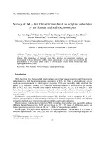
... 13000 CuO(111) 140 00 Cu2O(111) CuO(002) 15000 7000 6000 -550 mV 5000 40 00 -40 0 mV 3000 2000 -250 mV 1000 28 30 32 34 36 38 40 42 44 46 48 50 2 (deg) Fig 13 XRD pattern of thin films electrodeposited ... c) 40 0 C 0.06 d) 500 C CuO Cu2O 0.08 0.02 0.00 28 30 32 34 36 38 40 42 44 2 (deg) Fig X-ray diffraction patterns of electrodeposited Cu2O thin films a) as grown and annealed at b) 150 oC, c) 40 0 ... Cu2O thin film annealed at 500˚C 102 Solar Cells – Thin- Film Technologies Fabrication and characterisation of CuO/Cu2O heterojunction In order to fabricate CuO/Cu2O thin film hetorojunction, thin...
Ngày tải lên: 19/06/2014, 11:20

High depth resolution rutherford backscattering spectrometry with a magnet spectrometer implementation and application to thin film analysis 4
... V′1 ′ V′3 ′ V3 V 4 ′ V V′5 ′ V′2 ′ ′ V1′ − V2 gu ′ V′ − V4 By = gu ′ V′ − V6 Bz = gu Bx = V4 V′6 ′ V2 x V5 Fig 4. 20 Schematic of calculations of B field components , i = 1,2,3 ,4, 5,6 Chapter Analytical ... calibration as well as the spectrum conversion 12000 CompoundSP FORBIN Mathematica Counts 8000 40 00 41 0 44 0 47 0 500 Energy (keV) Fig 5.9 Comparison between energy spectrum obtained using FORBIN and ... 4. 8 Direct, Matrix, Numerical calculations and Experimental data 200 Experimental 150 Analytical Matrix Position Channels 100 SIMION 50 -50 -100 -150 -200 0.92 0.96 1. 04 1.08 Epsilon Fig 4. 24...
Ngày tải lên: 14/09/2015, 08:44

Metallic thin film on sige si substrates 4
... 0.6 0 .4 0.2 0 20 40 60 80 100 120 140 160 X [nm ] (b) 1.6 1 .4 1.2 Z[nm] (b) 0.8 0.6 0 .4 0.2 0 20 40 60 80 100 120 140 160 X[nm] 1.6 1 .4 1.2 Z[nm] (c) 0.8 0.6 0 .4 0.2 0 20 40 60 80 100 120 140 160 ... 75%Ni x1.2 65%Ni x1.3 x1.5 56%Ni x1.6 44 %Ni x1.9 30%Ni x2.7 19%Ni x4.2 858 856 8 54 852 Binding Energy (eV) 850 85%Ni x8 .4 75%Ni x4.8 65%Ni x3.3 56%Ni x2.7 44 %Ni x2.0 30%Ni x1.5 19%Ni x1.3 Pure ... 70 70 Atomic Ratio (%) 100 90 Atomic Ratio (%) 100 60 50 40 30 60 50 40 30 20 20 10 10 0 20 40 60 80 100 120 140 160 20 40 60 100 120 140 160 (b) (a) 100 90 90 80 80 70 70 Atomic Ratio (%) 100...
Ngày tải lên: 14/09/2015, 14:01
Tài liệu Báo cáo " Survey of WO3 thin film structure built on ito/glass substrates by the Raman and xrd spectroscopies" doc
... Weis, Matthias Wuttig, Thin solid films 41 4 (2002) 275 Toshikazu Nishide, Fujio Mizukami, Thin solid films 295 (1995) 212 A Elshafie, H.H Afify, A Abdel-All, phys stat sol (a) 1 74 (1999) 301 P.S Patil, ... Yianoulis, A Siokou, Thin solid films 3 84 (2001) 298 H.Y Wong, C.W.Ong, R.W.M Kwok, K.W Wong, S.P Wong, W.Y Cheung, Thin solid films 376 (2000) 131 I Porqueras, E Bertran, Thin solid films 377-378 (2000) ... 25 (2009) 47 -55 50000 (001) a) 800 WO 3/ ITO 300nm (200) 30000 20000 267.657 Intensity (cps) Intensity (a.u) 40 000 1000 802.5 14 W O 3/ ITO 300nm 701.7 14 130.857 10000 600 40 0 200 0 200 40 0 600...
Ngày tải lên: 13/02/2014, 03:20

Tài liệu MBA/SMA 0204, MBB/SMA 0207, MBE/SMA 0414 - Precision Thin Film Leaded Resistors pptx
... 0.01 ) no visible damage + 235 C; s solder bath method; SnPb40 4. 17 20 (Ta) Solderability 4. 22 (B4) Vibration 4. 16 4. 7 4. 25.3 4. 40 + 245 C; s solder bath method; SnAg3Cu0.5 h; 10 Hz to 2000 Hz ... www.vishay.com/doc?91000 MBA/SMA 02 04, MBB/SMA 0207, MBE/SMA 041 4 - Precision Precision Thin Film Leaded Resistors Current Noise A1 Vishay Beyschlag µV/V 0.1 MBE/SMA 041 4 MBB/SMA 0207 MBA/SMA 02 04 0.01 100 1K 10K ... MBA/SMA 02 04, MBB/SMA 0207, MBE/SMA 041 4 - Precision Precision Thin Film Leaded Resistors Vishay Beyschlag Power Dissipation P FUNCTIONAL PERFORMANCE MBE/SMA 041 4 MBB/SMA 0207 MBA/SMA 02 04 W 0.5...
Ngày tải lên: 20/02/2014, 10:20
Enhancement-Mode Metal Organic Chemical Vapor Deposition-Grown ZnO Thin-Film Transistors on Glass Substrates Using N2O Plasma Treatment docx
... time 305 sec 42 5 sec 665 sec 10 125 sec 10 34. 5° ZnO (0002) 35.3° ITO (40 0) 50.65° 60.25° ITO (44 0) ITO (622) As-grown N2O-treated - 14 10 -30 -20 -10 10 20 Gate Voltage, VGS (V) 30 30 40 50 60 70 ... (20 04) 45 6 32) R Menon, K Sreenivas, and V Gupta: J Appl Phys 103 (2008) 0 949 03 33) J H Kwon, J H Seo, S I Shin, and B K Ju: J Phys D 42 (2009) 065105 34) J Kanicki and S Martin: in Thin- Film ... 35.3° ITO (40 0) (b) -3 10 -5 10 Current (A) Intensity (arb unit) Corning Glass 34. 5° ZnO (0002) VGS = 15 V 50.65° 60.25° ITO (44 0) ITO (622) ID -7 10 -9 10 Gate Current -11 10 30 40 50 60 70...
Ngày tải lên: 05/03/2014, 21:20
gas sensing properties of metal - organics derived pt dispersed - tio2 thin film fired in nh3
... compositions of thin films were analyzed by SIMS Žsecondary ion mass spectroscopy Results and discussion The spin coated thin films were preheated at 40 08C in wet air and fired at 40 08C–5508C under ... of 40 08C–5508C In contrast, the gas sensitivity to 1000 ppm H greatly depended on the firing temperature The sensitivity became the maximum on the film fired at 45 08C The thin film fired at 45 08C ... Actuators B 67 (2000) 270–2 74 272 Table Relative resistance of the thin film fired in different atmosphere Žmeasured at 2008C Number Firing atmosphere Kind of thin film Kind of measuring gas Relative...
Ngày tải lên: 19/03/2014, 16:48
highly sensitive thin film nh3 gas sensor operating at room
... (1999) 47 8 48 5 [45 ] P Montmeat, R Lalauze, J.-P Viricelle, G Tournier, C Pijolat, Model of the thickness effect of SnO2 thick film on the detection properties, Sens Actuator B 103 (20 04) 84 90 [46 ] ... Carbon 41 (2003) 247 1– 247 6 [43 ] K Seo, K.A Park, C Kim, S Han, B Kim, Y.H Lee, Chirality- and diameter-dependent reactivity of NO2 on carbon nanotube walls, J Am Chem Soc 127 (2005) 157 24 15729 ... dioxide coated carbon nanotubes, Thin Solid Films 49 7 (2006) 355–360 [21] L Zhao, L Gao, Filling of multi-walled carbon nanotubes with tin(IV) oxide, Carbon 42 (20 04) 3251–3272 [22] B.-Y Wei, M.-C...
Ngày tải lên: 19/03/2014, 16:48
influence of polymerization temperature on nh3 response of pani tio2 thin film gas sensor
... (nm) 4 (nm) −10 10 20 30 857 8 74 859 865 840 42 5 42 3 41 5 41 8 42 3 366 363 369 360 330 399 390 378 371 359 Table Response time (T1 ) and recovery time (T2 ) of sensors based on PANI/TiO2 thin films ... PANI thin film prepared at 20 ◦ C and PANI/TiO2 nanocomposite thin films prepared at different polymerization temperatures ◦C 10 ◦ C 20 ◦ C T1 T2 T1 T2 T1 T2 23 47 70 94 117 141 6 70 68 44 50 33 ... 44 88 44 92 [4] X Zhang, G Yan, H Ding, Y Shan, Fabrication and photovoltaic properties of self-assembled sulfonated polyaniline/TiO2 nanocomposite ultrathin films, Mater Chem Phys 102 (2007) 249 –254...
Ngày tải lên: 20/03/2014, 13:04
modeling of the conduction in a wo3 thin film as ozone sensor
... properties of WO3 semiconductor material, Solid State Electron 45 (2001) 639– 644 [10] V.V Kissine, V.V Sysoev, S.A Voroshilov, Conductivity of SnO2 thin films in presence of surface adsorbed species, Sens ... O2 , O2 − , O or O− at 47 3 K and O or O− at 573 and 673 K) and ionized covering rate θ − (due to species O2 − or O− at 47 3 K and O− at 573 and 673 K) are given in Fig 4a and b, respectively We ... 1–16 [4] S.Z Karazhanov, Y Zhang, A Mascarenhas, S Deb, L.W Wang, Oxygen vacancies in cubic WO3 studied by first-principles pseudopotential calculation, Solid State Ionics 165 (2003) 43 49 [5]...
Ngày tải lên: 20/03/2014, 13:04
new technology of metal oxide thin film preparation for chemical sensor application
... 0.103 0.0 0.0 0 .46 3 0.303 0 .43 7 0.332 0.3 84 0 .44 9 Fig AFM surface morphology of WO3 thin films without interruption (a), one (b) and three (c) interruptions of the deposition process 3 .4 Discussion ... and 4, the sputtering process was interrupted once, two and three times, respectively A shutter was used to interrupt the deposition process The total deposition time was 40 , 40 .5, 41 and 41 .5 ... sensors, Sens Actuators 12 (1987) 42 5 44 0 [2] G Sberveglieri, S Groppelli, P Nell, V Lantto, H Torvela, P Romppainen, S Lepp¨ vuori, Response to nitric oxide of thin and thick a SnO2 films containing...
Ngày tải lên: 20/03/2014, 13:05
sensitivity properties of a novel no2 gas sensor based on mesoporous wo3 thin film
... Lett (1990) 44 1 44 4 [20] C Xu, J Tamaki, N Miura, N Yamazoe, Relationship between gas sensitivity and microstructure of porous SnO2 , Denki Kagaku (Electrochemistry) 58 (1990) 1 143 –1 148 L.G Teoh ... Langmuir 15 (1999) 1 748 –1753 [6] H.T Sun, C Cantalini, Microstructural effect on NO2 sensitivity of WO3 thin film gas sensors Part Thin film devices, sensors and actuators, Thin Solid Films 287 (1996) ... B (1991) 147 –155 [22] X Wang, S.S Yee, W.P Carey, Transition between neck-controlled and grain-boundary-controlled sensitivity of metal-oxide gas sensors, Sens Actuat B 24 (1995) 45 4 45 7 [23]...
Ngày tải lên: 20/03/2014, 13:07

thin film polypyrrole swcnts nanocomposites-based nh3 sensor
... ppm NH3 1.65 1 .45 an 1.0 1.35 24 27 30 33 36 39 42 45 48 51 o Operating temp ( C) Page 29 of 31 (a) 22 40 0ppm 20 NH3 220ppm 140 ppm 16 80ppm 14 an R(M) 18 300ppm 40 ppm 10ppm 12 200 40 0 Air M 10 ... literatures Response time (sec) 240 60 840 6000 References This work [45 ] [46 ] [48 ] [49 ] 202 120 1800 43 200 Ac ce pt ed M an us cr PPY/SWCNT PPY thin film SWCNTs film Single wire of PPY Single ... Response (Rg/Ra) 2.0 Ac ce 1 .4 1.2 0.0 0.8 1.6 2 .4 3.2 4. 0 4. 8 5.6 SWCNTs content (%) Page 27 of 31 Figure 2 .4 2.0 1.8 ip t 2.2 150 ppm NH3 cr 1.6 1 .4 1.2 1.0 0.8 200 40 0 600 800 1000 an us Response...
Ngày tải lên: 20/03/2014, 13:11

tio2 thin film gas sensor for monitoring ammonia
... 1979;86: 335 44 [20] Hahn SH, Bârsan N, Weimar U, Ejakov SG, Visser JH, Soltis RE CO sensing with SnO2 thick film sensors: role of oxygen and water vapour Thin Solid Films 2003 ;43 6:17– 24 ... planar structure thin film gas sensor was fabricated with TiO2 as the sensing layer A thin sensitive TiO2 6 84 B Karunagaran et al / Materials Characterization 58 (2007) 680–6 84 film was deposited ... deposition of TiO2 films using DC magnetron sputtering and the characterization of the films for gas sensing applications Experimental 2.1 Film preparation Titanium oxide thin films were deposited...
Ngày tải lên: 20/03/2014, 13:11

wet process-based fabrication of wo3 thin film for no2 detection
... of WO3 thin films Thin films of WO3 could be derived from the WO3 ·2H2 O sol added with PEG (2 wt.%) by one time spin coating and calcination at 300 ◦ C for h Fig shows SEM images of the thin films ... dry air for WO3 thin film devices, derived from WO3 ·2H2 O sols different in PEG content and calcined at 300 ◦ C (a) and 40 0 ◦ C (b) PEG content in mass%: (1) 2, (2) 7, (3) 15 and (4) 20 of the thick ... using a thick film of gold-loaded tungsten oxide, Chem Lett (19 94) 335 [4] G Sberveglieri, L Depero, S Groppelli, P Nelli, WO3 sputtered thin film for NOx monitoring, Sens Actuators B 26/27 (1995)...
Ngày tải lên: 20/03/2014, 13:11

wo3 thin film sensor prepared by sol–gel technique and its low-temperature sensing properties to trimethylamine
... He, Thin Solid Films 3 04 (1997) 13 [7] T Mochida, K Kikuchi, T Kondo, H Ueno, Y Matsuura, Sensors and Actuators B 24/ 25 (1995) 43 3 [8] S Manorama, G Sarala Devi, V.J Rao, Appl Phys Lett 64 (19 94) ... survey scan spectrum of the sample is shown in Fig 2(a) The peaks of tungsten 4p1/2 , 4p3/2 , 4d3/2 , 4d5/2 , 4f5/2 , 4f7/2 and oxygen 1s (O 1s) can be detected in the spectrum The photoelectron ... 10 (1993) 229 [4] G Sberveglieri, P Benussi, G Coccoli, S Groppelli, P Nelli, Thin Solid Films 186 (1990) 349 [5] L Bruno, C Pijolat, R Lalauze, Sensors and Actuators B 18/19 (19 94) 195 [6] C.H...
Ngày tải lên: 20/03/2014, 13:12
Báo cáo "Investigation of zinc oxide thin film by spectroscopic ellipsometry " ppt
... data analysis: measured versus calculated quantities, Thin Solid Films 3133 14 (1998) 33 [6] R Swanepoel, Ellipsometry data for some thin film samples, J Phys E: Sci Instrum., 16 (1983) 1215 [7] ... single film on the surface By regularly increasing complexity, we have constructed more complicated model, for instant, increasing the amount of possible films or the possible elements exist in film ... coefficient k on wavelength of ZnO film, illustrated in Fig 10 The ZnO film refractive indices in the wavelength range of 500 nm – 1100 nm were found to be from 1. 94 to 1.85 The extinction coefficient...
Ngày tải lên: 28/03/2014, 13:20

MBA/SMA 0204, MBB/SMA 0207, MBE/SMA 0414 - Professional Thin Film Leaded Resistors docx
... ) Note (1) ± (0 .4 % R + 0.05 ) for MBE/SMA 041 4 (2) ± (0.8 % R + 0.05 ) for MBE/SMA 041 4 (3) ± (0.2 % R + 0.05 ) for MBE/SMA 041 4 (4) ± (0 .4 % R + 0.05 ) for MBE/SMA 041 4 www.vishay.com ... heat, cyclic 4. 23.3 30 (Db) 4. 23 .4 (Aa) 4. 23.5 13 (M) 4. 23.6 30 (Db) Damp heat, cyclic - Short time overload 14 (Na) Rapid change of temperature 4. 13 4. 19 Cold Low air pressure 4. 29 45 (XA) Component ... www.vishay.com/doc?91000 MBA/SMA 02 04, MBB/SMA 0207, MBE/SMA 041 4 - Professional Professional Thin Film Leaded Resistors Test Voltage Vishay Beyschlag 10 kV kV 100 V MBE/SMA 041 4 MBB/SMA 0207 MBA/SMA 02 04 10 V 10 Ω...
Ngày tải lên: 31/03/2014, 00:20

Thin-Film RF/Microwave Capacitor Technology.
... 47 46 46 46 46 45 45 45 43 42 44 45 47 48 47 47 46 45 47 49 51 49 46 44 44 43 42 35 23 12 NA NA NA NA NA NA NA NA NA 4. 73 4. 87 5.01 5.16 5.30 5 .44 5.59 5.73 6.30 7.02 8.11 9.19 10.57 11.95 14. 23 ... 7 54 747 740 732 725 718 711 7 04 696 689 682 675 668 660 653 646 639 632 6 24 617 610 597 5 84 571 557 544 531 518 507 49 7 48 6 47 5 46 5 45 4 44 3 43 3 42 2 41 2 40 1 390 48 4 48 0 47 5 47 1 46 7 46 2 45 8 45 4 45 0 ... 44 43 44 44 45 45 45 45 44 44 44 44 45 44 43 42 42 41 41 37 32 28 27 28 28 29 30 31 33 34 40 4. 42 4. 55 4. 67 4. 79 4. 92 5. 04 5.16 5.29 5.78 6 .40 7.26 8.12 9.17 10.22 11.75 13.28 14. 98 16.68 18.83...
Ngày tải lên: 15/04/2014, 14:33
Thin film materials technology
... 5.1.3.2 PLZT Thin Films 271 5.1 .4 Perovskite Superconducting Thin Films .295 5.1 .4. 1 5.1 .4. 2 5.1 .4. 3 5.1 .4. 4 5.1 .4. 5 5.1 .4. 6 Studies of Thin Film Processes 301 Basic Thin Film Processes ... Nitride Thin Films 343 5.2.3 Si-N Thin Films 344 CARBIDES AND SILICIDES . 345 5.3.1 SiC Thin Films . 346 5.3.2 Tungsten Carbide Thin Films 355 5.3.3 Mo-Si Thin Films ... of Contents Thin Film Materials and Devices .1 1.1 THIN FILM MATERIALS 1.2 THIN FILM DEVICES 10 REFERENCES 14 Thin Film Processes 17 2.1 THIN FILM GROWTH PROCESS...
Ngày tải lên: 23/04/2014, 19:19