Optoelectronics Materials and Techniques Part 14 doc

Optoelectronics Materials and Techniques Part 14 doc
... 2 and an increase in the intensities of the 2100-cm -1 -infrared-absorption bands (see Fig. 4a and 1100-cm -1 -infrared-absorption bands (see Fig.4b). Optoelectronics - Materials and Techniques ... temperature (T d ). (a) As- deposited and (b) After two months air exposure Optoelectronics - Materials and Techniques 402 Table 2. Growth parameters and (002) F...
Ngày tải lên: 19/06/2014, 11:20

Optoelectronics Materials and Techniques Part 3 docx
... – quasi-particle that describes the collective movement of the lattice constituents. The phonons are characterized by energy and momentum (impulse) Optoelectronics - Materials and Techniques ... states and luminescence in porous silicon quantum-dots: the role of oxygen. Phys. Rev. Lett. 82,197-200 Optoelectronics - Materials and Techniques 72 spin density is abou...
Ngày tải lên: 19/06/2014, 11:20

Optoelectronics Materials and Techniques Part 4 docx
... temperatures coupled with wide bandgap has made GaN an attractive material for device operation in high temperature and caustic environments. Optoelectronics - Materials and Techniques 96 Augusts ... large lattice and thermal mismatches between nitrides and substrate. These stacking irregularities are also known as double positioning boundaries. Optoelectronics - M...
Ngày tải lên: 19/06/2014, 11:20
Optoelectronics Materials and Techniques Part 13 docx
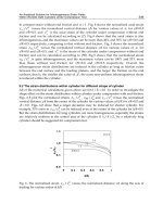
... which x and y are varied as described in Table 362 Optoelectronics - Materials and Techniques Optoelectronics - Materials and Techniques 354 Singh, J. (1992). Physics of Semiconductors and ... remarkable progress has been achieved (Hirayama (2005); Zhang et al. (2011)) and 14 Optoelectronics - Materials and Techniques 350 Fig. 7. The normalized st...
Ngày tải lên: 19/06/2014, 11:20
Optoelectronics Devices and Applications Part 14 docx
... of particles of fuel and accelerates their ignition by that more intensively, than more small particles and then more their section of absorption of radiation; Optoelectronics – Devices and ... R.A. (2009). Emission Spectrums and Radiative Heatexchange Mediums, Flames and Firing Chamber, In: Technics and Technology in XXI-th Century: Modern Conditions and Prospects of D...
Ngày tải lên: 19/06/2014, 11:20
Optoelectronics Materials and Techniques Part 1 pptx
... Polymeric Materials 187 Luigi Angiolini, Tiziana Benelli, Loris Giorgini, Attilio Golemme, Elisabetta Salatelli and Roberto Termine Optoelectronics - Materials and Techniques ... light- induced degradation.” Optoelectronics - Materials and Techniques 16 By applying Yelon’s treatment to e-h pairs generated by beta particles...
Ngày tải lên: 19/06/2014, 11:20

Optoelectronics Materials and Techniques Part 2 pptx
... refractive Optoelectronics - Materials and Techniques 36 and by using the current density in the ECD method. For the purpose of obtaining high- concentration Er-doped SRO materials (more ... wave nn θθ θθ ⎧ ⎛⎞ ⎪ ⎜⎟ − ⎪ ⎝⎠ = ⎨ ⎛⎞ ⎪ ⎜⎟ ⎪ − ⎝⎠ ⎩ (5) And the propagation matrix P m can be written by: 0 0 mx m mx m ik h m ik h e P e − ⎛⎞ ⎜⎟ = ⎜⎟ ⎝⎠ (6) Optoelectronics -...
Ngày tải lên: 19/06/2014, 11:20

Optoelectronics Materials and Techniques Part 5 pot
... to 3D island formation on the Si x N y -treated GaN surface and Optoelectronics - Materials and Techniques 124 continuous layer (Chen et al., 1999). Epitaxial lateral overgrowth and its ... INSPEC, London, U.K. Optoelectronics - Materials and Techniques 132 Liu,L., & Edgar, J.H. (2002). Substrates for gallium nitride epitaxy. Materials Science and Eng...
Ngày tải lên: 19/06/2014, 11:20

Optoelectronics Materials and Techniques Part 6 ppt
... gallery mode, where the direction of the 142 Optoelectronics - Materials and Techniques Cuprous Oxide (Cu 2 O): A Unique System Hosting Various Excitonic Matter and Exhibiting Large Third-Order Nonlinear ... prepared at 1148 K with iodine as a reactive agent. The prepared compound was yellow in colour. In the present work, the substrates are silicon (100) and Optoelectronics...
Ngày tải lên: 19/06/2014, 11:20

Optoelectronics Materials and Techniques Part 7 pptx
... views (Ti plate (a); foil (b)) and bottom side views (Ti plate (c); foil (d))] and XRD patterns [Ti plate (e and g) and Ti foil (f and h)] of anodized Ti plate and Ti foil. Figure 11(e-h) shows ... temperature of the material and a high value of Tg, well above the room temperature, is required. The NLO response is Optoelectronics - Materials and T...
Ngày tải lên: 19/06/2014, 11:20