light from the light emitting diode

Báo cáo sinh học: " Influence of helium-ion bombardment on the optical properties of ZnO nanorods/p-GaN light emitting diodes" pot
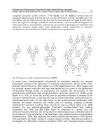
... The EL spectra reveal the same blue shift in the green emission as observed from the PL spectra The irradiation has a minor effect on the color-rendering properties of the LEDs It decreases the ... coated on the ZnO NRs to fill the gaps between the NRs to isolate electrical contacts on the ZnO NRs from reaching the p-type substrate and helps to prevent the carrier cross talk among the nanorods ... powder (99.9%) is used as the source material The pure zinc powder was placed in a quartz tube and the substrates are placed on the boat at the downstream side of the gas flow The substrates are placed...
Ngày tải lên: 18/06/2014, 22:20

báo cáo hóa học:" Influence of helium-ion bombardment on the optical properties of ZnO nanorods/p-GaN light emitting diodes" pdf
... The EL spectra reveal the same blue shift in the green emission as observed from the PL spectra The irradiation has a minor effect on the color-rendering properties of the LEDs It decreases the ... coated on the ZnO NRs to fill the gaps between the NRs to isolate electrical contacts on the ZnO NRs from reaching the p-type substrate and helps to prevent the carrier cross talk among the nanorods ... powder (99.9%) is used as the source material The pure zinc powder was placed in a quartz tube and the substrates are placed on the boat at the downstream side of the gas flow The substrates are placed...
Ngày tải lên: 20/06/2014, 04:20

Báo cáo hóa học: " Effect of triplet multiple quantum well structures on the performance of blue phosphorescent organic light emitting diodes" potx
... by the bipolar property of the CCLs Background Due to their high efficiency, phosphorescent organic light- emitting diodes [PHOLEDs] are promising light- emitting materials in organic light- emitting ... organic light- emitting diodes [PHOLEDs] Four types of devices from one to four quantum wells are fabricated following the number of CCLs which are mixed p- and n-type materials, maintaining the thickness ... improved for lighting applications Light emission in PHOLEDs depends on the properties of the organic material in the devices [3, 4] In particular, the energy level of the charge transport, host, and...
Ngày tải lên: 20/06/2014, 23:20
Báo cáo hóa học: " The origin of the red emission in n-ZnO nanotubes/p-GaN white light emitting diodes" pdf
... layer was then spun coated on the ZnO NTs to fill the gaps between the nanotubes with a view to isolate electrical contacts on the ZnO NTs to prevent them from reaching the p-type substrate, thereby ... muffin-tin orbital method, the calculated energy level of the Vo in ZnO is 1.62 eV below the conduction band [20] Hence, the energy interval from the V o energy level to the top of the valence band is ... helping to prevent the carrier cross talk among the nanotubes To form the top contacts, the tip of the ZnO NTs were exposed using plasma ion-etching technique after the deposition of the insulating...
Ngày tải lên: 21/06/2014, 05:20
Investigation of Mg doping profile in the pcladding layer for highbrightness AlGaInPbased light emitting diodes.
... the p-cladding layer The layer As the [Cp2 Mg]/[III] value in the “b” zone was inset in (b) shows the relative increase of brightness for the same LEDs increased from × 10−4 to × 10−4 , the light ... the oversaturated material problem.9 These results indicate that the hole concentration at the “b” zone in the p-cladding layer is directly influenced by improvement in the spontaneous light- emitting ... enhance the hole injection into the active Table I presents the detailed Mg doping profiles for region.7 The RIP decrease in the Test LED structure indithe three zones of the p-cladding layer in the...
Ngày tải lên: 31/07/2015, 18:48

Tài liệu INFRARED’ LIGHT-EMITTING DIODE APPLICATION doc
... Application Note The infrared light emitted from the LED of the photointerrupter is dispersed by particles of smoke The dispersion of light is s ensed by the light detector of the photointerrupter ... the LED in the linear region of the light- emitting characteristics In the arrangement of Figure 10, a fixed bias (IF1) is applied to the LED using R1 and R2 so that the maximum amplitude of the ... Circuits VCC When the switch is in the ON-state, the SCR2 and SCR3 turn on to discharge capacitor C4 so that the xenon lamp is energized to emit light The anode of the SCR2 is then reverse-biased,...
Ngày tải lên: 23/12/2013, 00:16

ELD electroluminescent display LED light emitting diode
... on the server running the adapter Suite\CustomRFC.zip” 1-(2) Copy the transport file with the naming pattern K9*.BI1 from the installation directory on the computer running the adapters to the ... SAP server) Extract from help(SAPAdapter.chm) “Installing the Custom RFCs for SAP ADO Provider” To install the RFCs 1-(1) Copy files from the computer running the adapters to the SAP application ... directory on the SAP application server: :\usr\sap\trans\cofiles 1-(3) Copy the transport file with the naming pattern R9*.BI1 from the installation directory on the computer running the adapters...
Ngày tải lên: 19/03/2014, 22:17

highly efficient blue organic light emitting diodes using quantum well like
... organic light- emitting diodes with blue -emitting Alq Photopolym Sci Technol 2004, 17:2 Reineke S, Lindner F, Schwartz G, Seidler N, Walzer K, Lüssem B, Leo K: White organic light- emitting diodes ... of organic light- emitting diodes Acta Phys Sin 2010, 59:8093 23 Jian Z, Juan G, Zhuo G, Ke D, Jiule C: An organic light- emitting device with ultrathin quantum-well structure as light emitting layer ... between the central and surrounding emitting layers The effect of layer thickness and combination of different emissive layers on charge carrier transport mechanism from the quantum well-like and the...
Ngày tải lên: 06/05/2014, 08:55
Organic Light Emitting Diode Material Process and Devices Part 1 pot
... that the iridium unit in 10 and 12 has the similar structure to 14 The appearance of the signal at 8.7 in the spectra for the products indicated that the free pyridyl group at the end of the ... mainly from the host polymer 16 in device F The behavior was different from the devices T and U, in which the luminescence from the doped platinum complex (605 and 650 nm) into 16 was detected These ... in the solutions were comparable For example, red luminescence from was observed and the wavelength at the maximum intensity was 620 nm The PL spectra for showed the emissions at ~620 nm from the...
Ngày tải lên: 19/06/2014, 21:20
Organic Light Emitting Diode Material Process and Devices Part 2 pptx
... occur in the UV region Furthermore, molecular systems that are light emitters in the visible region are potentially useful in the fabrication of organic light emitting diodes (OLEDs) Therefore, ... Synthesis and Photophysical Properties of Pyrene-Based Multiply Conjugated Shaped Light- Emitting Architectures: Toward Efficient Organic -Light- Emitting Diodes 27 interaction in the solid state The ... pyrene-cored light- emitting monomers (10-20) Although the IR spectra of 15 in the B- and G-form were essentially the same, and the lowershifted peak of the amide NH stretching at 3282 cm-1 indicated the...
Ngày tải lên: 19/06/2014, 21:20
Organic Light Emitting Diode Material Process and Devices Part 3 doc
... 64 Organic Light Emitting Diode – Material, Process and Devices injection from the electrodes in the OLED devices or through the dissociation of EHPs created by the incident light in the solar ... further confirming the above results that the incorporation of trimethylsilyl groups into the polymeric backbone decreases the interactions between the pyrene units On the other hand, the band around ... at the 1,3-positions in the monomer synthesis, and also for both attaining sufficient solubility and avoiding the use of long alkyl chains The UV-vis absorption and 50 Organic Light Emitting Diode...
Ngày tải lên: 19/06/2014, 21:20

Organic Light Emitting Diode Material Process and Devices Part 4 pdf
... exceeding the potential to overcome the HOMO-LUMO energy gap in the active material of the OLED, irrespective of the energy levels of the electrodes The SOC effects on the T1 - S0 transition in the ... means that the nonradiative quenching of the T1 state is faster in the latter complexes Therefore in the meridional isomer the SOC matrix element together with the difference between the permanent ... Similar to other Ir(III) complexes, the HOMOs are mainly localized on the metal center and the phenyl ring of the ppy ligands while the LUMOs are delocalized mostly on the pyridine part of the ppy...
Ngày tải lên: 19/06/2014, 21:20
Organic Light Emitting Diode Material Process and Devices Part 5 ppt
... device C, the emission of red light may be originated from the direct electron capturing from the host and recombining at holes trapped at the HOMO of the dopant in the emitting layer Indeed, the hole ... Organic Light- Emitting Diodes with Simple Structure 109 can over-flow in the Bepp2 CCL, creating more excitons in the double QW structure Therefore, the device D with the Bepp2 CCL improves the recombination ... Bässler 2009) The photoexcited state in one material diffuses to the interface of the other where dissociation occurs The size of the phase separation between the two materials should be on the same...
Ngày tải lên: 19/06/2014, 21:20

Organic Light Emitting Diode Material Process and Devices Part 6 ppt
... Förster transfer from the excited triplet S1 state of the host to the excited triplet S1 state of the guest and Dexter transfer from the excited triplet T1 state of the host to the excited triplet ... Organic Light- Emitting Diodes with Simple Structure 121 In m-MTDATA, no barrier for hole injection from the surface treated ITO (5.1 eV) to the HOMO (5.1 eV) of the m-MTDATA exists Further, this ... level matches with the HOMO (5.1 eV) of the Ir(piq)3 While, electrons injected from the cathode move freely on the LUMO energy of Bebq2 In case of the device B, the HOMO energy in the α-NPB material...
Ngày tải lên: 19/06/2014, 21:20
Organic Light Emitting Diode Material Process and Devices Part 7 ppt
... assigned to the long axis of the molecules, which are aligned vertically on the surface However, in the case of the PTCDI-C8H films with the NPD interfacial layer, the diffraction peaks are rather weak, ... at the interface between the hole-transporting layer and the n-type semiconductor film The role of the interfacial layer can be basically attributed to the separation of the channel carriers from ... be discussed from the viewpoint of electronic interaction between the hole transporting layer and the n-type channel layer In the single layer device 152 Organic Light Emitting Diode – Material,...
Ngày tải lên: 19/06/2014, 21:20

Organic Light Emitting Diode Material Process and Devices Part 8 potx
... to their corresponding PL spectra Take into account the fact that the exciton disassociates easily under the excitation of electric field than the light, red shifting of 174 Organic Light Emitting ... presents the driving voltage and the efficiency at luminance 100 and 200 cd/m2 in dependence on the thickness of BCP It is seen that despite of the higher voltage of the 184 Organic Light Emitting Diode ... confine the holes (due to the high hole barrier from 0.7 eV at the EML/HBL (Fig.29) thus improving the recombination at the EML/BCP interface, but on the other hand they aren’t enough dense to...
Ngày tải lên: 19/06/2014, 21:20
Organic Light Emitting Diode Material Process and Devices Part 9 pptx
... resulted in the transfer of the Alq3 material from the donor substrate to the receptor substrate The “UCB” and “LTL” letters were formed from combining the 0.9×0.9 206 Organic Light Emitting Diode ... apart in the vacuum chamber And then the glass donor is put on the substrate and fixed by the clamping equipment It is moved out of the chamber onto the stage of the laser transfer system in the atmosphere ... into the chamber The 200 Organic Light Emitting Diode – Material, Process and Devices transfer gap between the glass donor and the substrate is precisely controlled all over the substrate by the...
Ngày tải lên: 19/06/2014, 21:20
Organic Light Emitting Diode Material Process and Devices Part 10 ppt
... etchant The system will spin the wafer while the etchant is sprayed over the wafer, causing the etching of the silver The main issue with this system is to find a good rotation speed for the spinner ... oxygen These properties therefore would be very useful when it comes to protecting the pentacene from degrading Also the deposition technique is fully compatible with the semiconductor, since the ... on the surface energy of the resulting film and therefore on the adhesion of subsequent layers Previous research has shown that the more chlorine atoms that are bonded on the benzene ring, the...
Ngày tải lên: 19/06/2014, 21:20

Organic Light Emitting Diode Material Process and Devices Part 11 doc
... 2007) The decrease in the resistivity of the IAI films may be caused by the increase in the carrier density of the IAI films, which results from the presence of the Au interlayer However, the ITO/Au/ITO ... visible light range The spectrum of 200oC shows the lowest transmittance The color of the film was dark violet, but the others were blue Light scattering by the rough surface reduced the transmittance ... general, the brightest diodes with the higher current densities decayed the most rapidly; however, the diodes with the ITO in the device structure continued to decay more rapidly even when the current...
Ngày tải lên: 19/06/2014, 21:20
Organic Light Emitting Diode Material Process and Devices Part 12 pptx
... complying with the user’s need The other variation is found in the indexing of the array variable The initial index of the array in MATLAB is instead of 0, which is different from Eq The main calculation ... between them The results are plotted using “plot” function and the reflectivity of the multi-layers is calculated from the E0 and E0’ 0 0.05 0.1 0.15 0.2 0.25 0.3 0.35 Fig The output from the execution ... annotation at the bottom of the plot between the circular marks, which represent the boundaries of each layer The light is supposed to be incident on the overcoat layer first In the design of the OLED...
Ngày tải lên: 19/06/2014, 21:20