devices hosts and applications
Optoelectronics Devices and Applications Part 1 pdf
... PPV devices, both single carrier and dual carrier devices, paved the way to the better understanding of mobility of electrons and holes Electron only devices are fabricated by a PPV layer sandwiched ... discussed design and fabrication of device structures and the underlying phenomena Many of the optoelectronic and photonic effects are integrated into a vast array of devices and applications in ... technology and even in entertainment, data storage, and holography The wide range of such applications in the field of optoelectronics and photonics ensures that it is generally a well-funded and thriving...
Ngày tải lên: 19/06/2014, 11:20

Optoelectronics Devices and Applications Part 2 potx
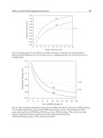
... mid-bandgap level between the conduction band and the valence band The maximum density distribution (electrons per energy levels) is around to 1.8 eV (Snyman 2010a) , and relaxation to mid-bandgap ... Dilute-Nitride Optoelectronic Devices SPSLs and and Dilute-Nitride Optoelectronic Devices well and explained it quantitatively by nitrogen diffusion out of the quantum well On the other hand, Buyanova et ... group III elements and separation of In and N into distinct, separate, layers 61 11 SPSLs Dilute-Nitride Optoelectronic Devices SPSLs and and Dilute-Nitride Optoelectronic Devices Hong et al...
Ngày tải lên: 19/06/2014, 11:20
Optoelectronics Devices and Applications Part 3 ppt
... equation and/ or Dirac equation and a few of parameters unrelated to specific 108 Optoelectronics – Devices and Applications materials, namely, electron mass m and charge e; atomic mass M and charge ... interstitial and substitutional nitrogen in GaN x As1x , Applied Physics Letters 80: 2314–2316 SPSLs Dilute-Nitride Optoelectronic Devices SPSLs and and Dilute-Nitride Optoelectronic Devices 73 ... Optoelectronics – Devices and Applications Will-be-set-by-IN-TECH Gilet, P., Chevenas-Paule, A., Duvaut, P., Grenouillet, L., Hollinger, P., Million, A., Rolland, G & Vannuffel, C (1999) Growth and characterization...
Ngày tải lên: 19/06/2014, 11:20

Optoelectronics Devices and Applications Part 4 pptx
... three conduction band bottom energy not only indicates the Si, Ge and Sn conduction band bottom are located at ( near) X, L and Γ point ( α-Sn is already a zero band gap materials ) and more, it indicates ... direct 114 Optoelectronics – Devices and Applications bandgap in normal pressure In addition, I-VII group Ag halide, AgCl and AgBr have Oh symmetry though they are indirect band gap material The only ... conduction band bottom and the valence band top Nevertheless, the main features of both the electronic structure and the band gap type are dominantly determined by crystal structure and their crystal...
Ngày tải lên: 19/06/2014, 11:20
Optoelectronics Devices and Applications Part 5 pot
... frequency band and higher detectivity (D*) Because of the many advantages, MCT photodetectors are frequently used in cavity enhanced applications 168 Optoelectronics – Devices and Applications ... These and other devices (e.g wheelchairs, incubators, power injectors to deliver drugs and contrast agents, and interventional devices such as catheters) cover a wide range of functions and electromechanical ... alignment and their firing characteristics The frequency range of EEG signals is from to 100 Hz and can been deconstructed into different frequency bands 176 Optoelectronics – Devices and Applications...
Ngày tải lên: 19/06/2014, 11:20

Optoelectronics Devices and Applications Part 6 pptx
... and intensities of 14 NH3 hot bands in the 5-8μm (3v2 - v2 , v2 + v4 - v2 ) and 4μm (4v2 - v2 , v1 - v2 , v3 - v2 ) regions, J.Mol.Spectrosc 209: 30–49 202 14 Optoelectronics – Devices and Applications ... molecule−1 This is around one thousand times greater than was the case in the Applications and Optoelectronic of Ammonia of Detection of Ammonia Applications and Optoelectronic Methods of Detection ... light reflected from the earths atmosphere, and passed it though a pressure Applications and Optoelectronic of Ammonia of Detection of Ammonia Applications and Optoelectronic Methods of Detection...
Ngày tải lên: 19/06/2014, 11:20
Optoelectronics Devices and Applications Part 7 potx
... convention given 244 18 Optoelectronics – Devices and Applications Will-be-set-by-IN-TECH by Fig.18 where ΔV and ΔI are the input voltage and current respectively, and i L is the photonic current related ... 1.55μm VCSELs, the top and bottom DBR were grown as 28 and 38 pairs of undoped InAlGaAs/InAlAs layers And for the 1.3μm VCSELs, the top and bottom DBRs consisted of 33 and 50 layers respectively ... Au/Ni/Au 232 Optoelectronics – Devices and Applications Will-be-set-by-IN-TECH layers at the top and pairs of n-doped SiO/Si materials at the bottom The materials given a 1.3 and 1.5 μm wavelength are...
Ngày tải lên: 19/06/2014, 11:20
Optoelectronics Devices and Applications Part 8 pot
... Intersubband Transitions, in Intersubband Transitions in Quantum Wells: Physics and Device Applications I, Capasso, F and Liu, H C (eds.), Semiconductors and Semimetals, vol 62, 1-32 and 73-80, ... photodetector physics and novel devices, in Intersubband Transitions in Quantum Wells: Physics and Device Applications I, Capasso, F and Liu, H C (eds.), Semiconductors and Semimetals, vol 62, ... (olive), 80 Å (purple), and 100 Å (orange), respectively QW width and cap layer thickness are L w = 150 Å and Lc = 20 Å, respectively 282 Optoelectronics – Devices and Applications Therefore,...
Ngày tải lên: 19/06/2014, 11:20
Optoelectronics Devices and Applications Part 9 docx
... sink with ScD core and copper top and bottom layer 337 338 Optoelectronics – Devices and Applications Fig 11 Comparison of μ-PL measurement of a standard copper heat sink (left) and an expansion ... beam components Ex (x) and E y (x) so that each of them can be independently 318 Optoelectronics – Devices and Applications Fig Degree of coherence given by Eq (49) for and different values ... The bold-faced arrows and circled dots denote polarization directions 320 Optoelectronics – Devices and Applications Again disregarding the negligible changes of coherence and polarization properties...
Ngày tải lên: 19/06/2014, 11:20

Optoelectronics Devices and Applications Part 10 docx
... bandwidth and latency 2.3.4 Overview of bandwidth demand Table summarizes the different signals and their approximate net bandwidth Note that there is only a very limited variety of signal bandwidth ... fiber links and/ or colors is assumed 376 Optoelectronics – Devices and Applications Will-be-set-by-IN-TECH Bandwidth consumption Several models exist that consider the difference in bandwidth usage ... 380 12 Optoelectronics – Devices and Applications Will-be-set-by-IN-TECH FOR i=1 to n DO if (bw
Ngày tải lên: 19/06/2014, 11:20
Optoelectronics Devices and Applications Part 11 potx
... Switches and Routing Devices, D-06-2, pp.1-2 Part Signals and Fields in Optoelectronic Devices 20 Low Frequency Noise as a Tool for OCDs Reliability Screening Qiuzhan Zhou, Jian Gao and Dan’e ... development of the information and science, more and more newly semiconductor devices are used in the electronic equipments or systems, and so is the Optoelectronic Coupled Devices (OCDs) Because of ... piezoelectric properties: zincblende and wurtzite Silicon based semiconductors are not piezoelectric and will not be covered in this chapter 420 Optoelectronics – Devices and Applications Will-be-set-by-IN-TECH...
Ngày tải lên: 19/06/2014, 11:20
Optoelectronics Devices and Applications Part 12 pot
... Especially the low weight and the easy and economic handling make this kind of fiber the first choice But 452 Optoelectronics – Devices and Applications for now the data rates and the temperature range ... bandwidth is characterised by the fibers attenuation curve between 1300 nm and 1650 nm Here using 458 Optoelectronics – Devices and Applications POF the bandwidth ist allocated beween 400 nm and ... T., Yu, S F & Sun, X W (2006) Band parameters and electronic structures of Wurtzite zno and zno/mgzno quantum wells, Journal of 442 24 Optoelectronics – Devices and Applications Will-be-set-by-IN-TECH...
Ngày tải lên: 19/06/2014, 11:20
Optoelectronics Devices and Applications Part 13 pdf
... lengths of waves and a space angle within a hemisphere 488 Optoelectronics – Devices and Applications a) b) c) Fig 13 Spectral dependences of parameter βν in bands 1,37 (a), 1,87 (b) and 2,7 m (c) ... vibrational and rotational energy distribution which leads to anomalously high vibrational 496 Optoelectronics – Devices and Applications and rotational temperatures Increasing the pressure and introducing ... vicinity of lengths of waves 2,1 and 1,4 m, and for the basic electronic state they are in a vicinity of lengths of waves 1,43 and m 502 Optoelectronics – Devices and Applications Results of definition...
Ngày tải lên: 19/06/2014, 11:20
Optoelectronics Devices and Applications Part 14 docx
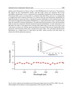
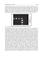
... mediums and flames have allowed to spend registration of spectra of absorption and spectra of radiation various flames with the average and high spectral 522 Optoelectronics – Devices and Applications ... can possibly be prolonged and 536 10 Optoelectronics – Devices and Applications Optoelectronics Fig Exponential and non-exponential photoelectric relaxations in multiple sandwich structures controlled ... Mass concentration of 524 Optoelectronics – Devices and Applications sooty ashes and its microstructure considerably depend on structure of gas fuel and a burning mode At performance of calculations...
Ngày tải lên: 19/06/2014, 11:20
Optoelectronics Devices and Applications Part 15 doc
... Optoelectronics – Devices and Applications producing ultra-compact, low power and high-sensitivity optical devices, towards the level of single photon detection and emission, and onwards to computation ... Fig The typical band structures of electronic and photonic crystals Fig Free space dispersion relations for photons (left) and electrons (right) 582 Optoelectronics – Devices and Applications Fig ... materials structures at nm length scales and their applications in general Waves in the form of electromagnetic and quantum mechanical, and materials as semiconductors and metals are the focus Different...
Ngày tải lên: 19/06/2014, 11:20
Optoelectronics Devices and Applications Part 16 docx
... bands exist for every direction and those ‘stop bands’ overlap within certain wavelength 592 Optoelectronics – Devices and Applications Fig 14 The constructive interference for the photonic band ... emission bands either appear due to radiative inter-band recombination of electrons and holes in the s-p and d bands, or originate from radiative intra-band transitions within the s-p band across ... (quantum dots), and (iii) size-dependent absorption and confinement is exploited in plasmonic solar cells and biosensing Metal 618 Optoelectronics – Devices and Applications nanoparticles and nanotips...
Ngày tải lên: 19/06/2014, 11:20

Optoelectronics Devices and Applications Part 17 potx
... 630 Optoelectronics – Devices and Applications Zhiyong, F.; Ruebusch, D J.; Rathore, A A.; Kapadia, R.; Ergen, O.; Leu, P W & Javey, A (2009) Challenges and Prospects of Nanopillar-Based ... ISSN 1998-0124 Zouhdi, S.; Sihvola, A & Vinogradov, A P (2009) Metamaterials and Plasmonics: Fundamentals, Modeling, Applications Springer, ISBN 978-1-4020-9405-7, Germany ...
Ngày tải lên: 19/06/2014, 11:20

Silicon Carbide Materials Processing and Applications in Electronic Devices Part 1 docx
... physical and chemical properties make silicon carbide (SiC) a prominent candidate for a variety of applications, including high-temperature, high-power, and high-frequency and optoelectronic devices, ... Processing and Applications in Electronic Devices and Perlado(Malerba, L & Perlado, J M., 2001) argued that both Frenkel pairs and antisite defects play significant roles in the amorphization process and ... 309 Piotr Klimczyk Part Silicon Carbide: Electronic Devices and Applications 335 Chapter 14 SiC Devices on Different Polytypes: Prospects and Challenges 337 Moumita Mukherjee Chapter 15 Recent...
Ngày tải lên: 19/06/2014, 11:20

Silicon Carbide Materials Processing and Applications in Electronic Devices Part 2 pot
... (a and c) in Å, carbon and silicon fractional coordinates (x, y, z), multiplicities and Wyckoff positions of the sites for selected clathrates I and II and sodalite Fig 13 Band structures and ... and Applications in Electronic Devices Will-be-set-by-IN-TECH Polk, D and Boudreaux, D (1973) Tetrahedrally Coordinated Random-Network Structure Phys Rev Lett 31,92–95 Pirouz, P., Chorey, C and ... structure of the Si(111) (2X1) surface Phys Rev B 54,1482–1485 Xu,G and Deng,B and Yu,Z and Tong,S.Y and Van Hove,M.A and Jona,F and Zasada,I (2004) AAtomic structure of the cleaved Si(111)-(21)...
Ngày tải lên: 19/06/2014, 11:20

Silicon Carbide Materials Processing and Applications in Electronic Devices Part 3 pdf
... Carbide – Materials, Processing and Applications in Electronic Devices Will-be-set-by-IN-TECH The reported phase stability between α(hexagonal) and β(cubic) might be 6H and 3C If this assumption is ... – Materials, Processing and Applications in Electronic Devices Will-be-set-by-IN-TECH Verma, A R & Krishna, P (1966) Polymorphism and polytypism in Crystal, John Wiley and Sons, New York Wesch, ... nanocrystalline film 70 Silicon Carbide – Materials, Processing and Applications in Electronic Devices containing cubic 3C and rhombohedral 21R, has a band emission with three peaks at 2.65, 2.83, 2.997 eV...
Ngày tải lên: 19/06/2014, 11:20