antireflection antistatic thin films for crts
Báo cáo hóa học: " Electrospray deposition of polymer thin films for organic light-emitting diodes" pot
... applicable to large-area device fabrication Much effort has been made for solution process development that can form nanoscale -thin organic films with a large area while minimizing material wastes ... performance made by the electrospray process The summary of device performances is in Table To investigate the difference between electrospray and spin-coating processes, PVK thin films were formed ... the electrospray process to organic thin films in OLEDs was demonstrated in small-scale devices [12] In this work, we demonstrated nanoscale-thick organic thin films using the electrospray process...
Ngày tải lên: 20/06/2014, 23:20
Báo cáo hóa học: "Synthesis and characterization of VO2-based thermochromic thin films for energy-efficient windows" pdf
... same conditions as for film preparation, but in an oxygen-free atmosphere This procedure ensures an oxide-free metallic surface for each deposition For the deposition of the films, both oxygen ... the elemental composition of the Table Processing conditions used for depositing the VO2 films W- and Mo-doped films Nb-doped films Base pressure (mbar) × 10-5 × 10⁻⁵ -3 × 10⁻³ Work pressure (mbar) ... achieved for Mo-doped and Nb-doped films, respectively The transition temperature (Tt) obtained for the pure VO2 film prepared by pulsed-DC sputtering was 59°C, which is lower than that obtained for...
Ngày tải lên: 21/06/2014, 04:20
Báo cáo hóa học: " Pd Nanoparticles and Thin Films for Room Temperature Hydrogen Sensor" potx
... typical X-ray diffraction patterns (XRD) for the sputtered Pd thin films Film thickness of 150 nm was same for sputtered thin films used for hydrogen sensing Grain size in the films was observed to ... 2008), p 1967 15 F Wu, J.E Morris, Thin Solid Films 246, 17 (1994) 16 Y.-T Cheng, Y Li, D Lisi, W.M Wang, Sens Actuators B: Chem 30, 11 (1996) 17 A Barr, Thin Solid Films 41, 217 (1977) 18 T Xu, M.P ... X-ray diffraction data and given in our previous article [22] Sputtering Deposition of Pd Thin Films Palladium thin films were prepared by DC-magnetron sputtering system on oxidized silicon substrate...
Ngày tải lên: 22/06/2014, 00:20
Preparation and characterization of ferroelectric thin films for tunable and pyroelectric applications
... associated with thin films are thought to have significant effects [21-23] Studies on ferroelectric thin films are therefore complicated The performance of a specific ferroelectric thin film is ... potential of BTS thin films The efforts toward improving the tunable and pyroelectric properties of BTS thin films have demonstrated the appealing prospective applications of BTS thin films in the relevant ... 2.1 Competing technologies for tunable circuits…………………… ….…26 Table 3.1 Deposition conditions for BTS thin films ……………………………39 Table 3.2 Properties of the BTS thin films with different thicknesses……………52...
Ngày tải lên: 10/09/2015, 15:48

A study of a fe2o3 thin films for the oxygen evolution reaction in water photolysis
... α-Fe2O3 thin films The synthesis of α-Fe2O3 thin films by a two-step process comprising the electrodeposition of thin iron films and the calcination of the iron films in air at 650℃ to form hematite ... 2θ (degrees) Fig 3.1 XRD patterns of (a) as-deposited iron thin films, (b) α-Fe2O3 thin films obtained from the as-deposited iron thin films after two hours of calcination in air at 650 oC (c) ... iron thin film, (b) cross-sectional view of α-Fe2O3 thin film formed by calcining the as-deposited iron thin film in air for two hours at 650oC, (c) and (d) the top views of the α-Fe2O3 thin...
Ngày tải lên: 26/09/2015, 10:05

Preparation of oriented molybdenum disulfide thin films for photoelectrochemical energy havesting applications
... for 1h for times to remove the excess lithium ions in the form of LiOH Finally, the suspension was centrifuged at 3000rpm for 0.5h for 3-4 times to remove the thicker materials MoS2 thin films ... of LTMDs in organic solvents Furthermore, atomically thin films of LTMDs can be synthesized by several other methods For instance, MoS2 thin films were successfully synthesized by annealing (NH4 ... does not allow the formation of large single crystals On the other hand, the synthesis of large area and highly-oriented LTMD thin films has been developed recently.3-5 These thin films offer an...
Ngày tải lên: 30/09/2015, 10:13

Báo cáo "Preparation and characteristics of the In-doped ZnO thin films and the n-ZnO:In/p-Si heterojunctions for optoelectronic switch" potx
Ngày tải lên: 14/03/2014, 13:20
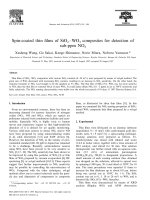
spin-coated thin films of sio2–wo3 composites for detection
... sensor for nitrogen oxides, J Electrochem Soc 141 (1994) 2207 – 2210 [4] G Sberveglieri, G Faglia, S Groppelli, P Nelli, Methods for the preparation of NO, NO2 and H2 sensors based on tin oxide thin ... WO3, WO3 + 5wt% SiO2, WO3 + 10wt% SiO2 and WO3 +20wt% SiO2 thin films deposited on alumina substrates with Au electrodes Fig AFM images of thin films (a): WO3, (b): SiO2 (20%)–WO3 X Wang et al / ... 0.4 ppm NO2 in air day for 10 days As shown in Fig 9, both Rg and Ra were fairly stable over the whole test period This confirms that the film is stable enough at least for a short term 3.4 Imprecation...
Ngày tải lên: 20/03/2014, 13:08
SOL-GEL TECHNOLOGY FOR THIN FILMS, FIBERS, PREFORMS, ELECTRONICS, AND SPECIALTY SHAPES potx
... Opto-Electronic Films Magnetic Films Barrier Films Sulfide Films Glassy Thick Films Unsupported Glass Films New Oxide-Based Gel Films Organic Modified Silicate Films Scuff ... are largely in the area of thin films These films have been developed for optical, mechanical and electrical applications About one-third of this book covers thin films The second area where ... Cataloging-in-Publication Data Sol-Gel technology for thin films, fibers, preforms, electronics, and speciality shapes Bibliography: p Includes index Ceramic materials Glass fibers Thin films Colloids I Klein, Lisa...
Ngày tải lên: 30/03/2014, 12:20

functional thin films and nanostructures for sensors. synthesis, physics, and applications
... Functional Thin Films and Nanostructures in Gas Sensing Audrey Nelson 85 Chemical Sensors: New Ideas for the Mature Field Radislav A Potyrailo 103 Applications of Functional Thin Films for ... respond? J Fortin GE Global Research Center Research Circle, KW C314, Niskayuna, NY12309 e-mail: fortinje@research.ge.com A Zribi and J Fortin (eds.), Functional Thin Films and Nanostructures for Sensors, ... Nanostructured Thin Films 37 Chemical Vapor Deposition Methods The chemical vapor deposition (CVD) technique is a widely used method for depositing thin films and nanostructures for a large variety...
Ngày tải lên: 04/06/2014, 15:14
Báo cáo hóa học: " Sol–Gel and Thermally Evaporated Nanostructured Thin ZnO Films for Photocatalytic Degradation of " doc
... degradation of 2,4,6-TCP The formed intermediates were determined and the degradation mechanism was discussed Experimental Work ZnO Thin Films by Thermal Evaporation Thin films of Zn were thermally ... starting materials and good chemical homogeneity of the product Therefore, sol–gel methods are very convenient for the preparation of thin films of high surface area amorphous oxide materials [24] Among ... its high surface reactivity [10] ZnO can be used in different forms, like single crystals, sintered pellets and thin films However, thin films have exhibited a wide variety of applications in environmental...
Ngày tải lên: 22/06/2014, 00:20

Growth and characterization of nickel oxide thin films and nanostructures for novel device applications
... structure for optimizing the device performance Additionally, NiO thin films fabricated by thermal oxidation of evaporated Ni film are also characterized for comparison with the sputtered films 2.1.2 ... Experimental Details .29 Growth of Thin Films and Nanowires 29 3.1.1 Sputtering for thin film growth 29 3.1.2 Chemical bath deposition for porous film growth 30 3.1.3 Anodization, ... with suitably uniform tube walls by oxidation of nickel nanowires was demonstrated for the first time The applications of NiO thin films and nanostructures were then investigated for resistive switching...
Ngày tải lên: 09/09/2015, 10:07
Tribological studies of ultra thin films at head media interface for magnetic data storage systems
... protective coatings films, DLC films have shown promising results to be used as a candidate for coating magnetic tape recording heads Among different types of DLC films, an ultra -thin tetrahedral ... low-cost information storage technology and has spanned the range of computing platforms from desktops to supercomputers For several decades, it has been unmatched in terms of price, performance ... Spratt of Hewlett-Packard and Dr Wayne Imaino of IBM for providing the required materials and equipments for this project and more importantly for their valuable advice, guidance and help in different...
Ngày tải lên: 09/09/2015, 10:17

Fabrication and characterisation of solid phase crystallised plasma deposited silicon thin films on glass for photovoltaic application
... flow ratios for the n-type poly-Si thin films obtained from SPC of PECVD a-Si:H films deposited at (a) 380°C and, (b) 410 °C Also shown, for comparison, is the Raman spectrum measured for a polished ... template for other earth abundant materials Poly-Si thin films have good stability and don’t degrade over time [14] In addition, doped poly-Si thin films are found to have very high mobilities for ... n-type poly-Si films on glass for thinfilm solar cell applications A sharp and high-quality interface is formed between 49 nm thick β-FeSi2(Al) and poly-Si through the formation of a thin layer (~7...
Ngày tải lên: 09/09/2015, 11:21

Application of biased scanning probe microscopy techniques for multifunctional characterization of bifeo3 and zno thin films
... to calculate the hardness of thin films from nanoindentation data”, 4th International conference on Technological Advances of Thin Films & Surface Coatings (ThinFilms2008), Singapore, July 13-16, ... Zinc Oxide (ZnO) thin film studied by Kelvin probe force microscopy (submitted for review) In addition, following papers are published based on mechanical properties of thin films, which are ... molecular beam epitaxy (MBE) are the common techniques for thin film sample deposition, which are also being used for multiferroic thin films Only a few classes of multiferroic materials, such...
Ngày tải lên: 10/09/2015, 08:41
Exchange bias characteristic in co pd n FEMN bi layered thin films with perpendicular anisotropy and the applications for spin valves in spintronics
... nm)/Ta exchange biased thin films before and after annealing at 3.3 kOe 83 Figure 4.9 XRD patterns of Si/Ta(2)/[Pd(0.6)/Co(0.23)] /FeMn(11.6 nm)/Ta exchange biased thin films before and after annealing ... PEB thin films for seed layer of Ta, Pd and Cu 100 Figure 5.2 XRD pattern of Si Si/Seed layer/[Pd(1.2)/Co(0.3)] /FeMn(12)/Pd(2 nm) exchange biased thin films with perpendicular anisotropy for ... nm)] /Ta multi-layered thin films, (b) Si/Ta(2)/FeMn(11.6)/[Co(0.23)/Pd(0.6 nm)] /Ta, (c) Si/Ta(2)/[Pd(0.6)/Co(0.23)] /FeMn(11.6 nm)/Ta exchange 88 x biased thin films before and after annealing...
Ngày tải lên: 10/09/2015, 15:53

Vapor phase polymerized thin films and seeding polymerized nanofibers membranes of poly (3,4 ethylenedioxythiophene) for optoelectronic applications
... Poly(3,4-ethylenedioxythiophene) Thin Films for Optoelectronic Applications ABTRACT Surface Morphology and Conductivity Control of Vapor-phase Polymerized Poly(3,4-ethylenedioxythiophene) Thin Films for Optoelectronic ... THESIS FOR THE DEGREE OF MASTER OF SCIENCE Advisor: Jae-Do Nam, Professor Vapor-phase Polymerized Thin Films and Seeding-polymerized Nanofibers Membranes of Poly(3,4-ethylenedioxythiophene) for ... vapor-phase polymerized poly(3,4-ethylenedioxythiophene) thin coating for flexible optoelectronic applications, Submitted to Thin Solid Films (2006) Thuy Le Truong, Youngkwan Lee, Hyouk Ryeol...
Ngày tải lên: 22/05/2016, 16:57

The Materials Science of Thin Films 2010 pptx
... of Thin Films 451 10.1 Introduction to Electrical Properties of Thin Films 451 Conduction in Metal Films 455 Electrical Transport in Insulating Films ... of Thin Film Preface xv Technology (1970) and Chopra, Thin Film Phenomena (1969), as well as more recent books on thin films, e.g., Pulker, Coatings on Glass (1984), and Eckertova, Physics of Thin ... for too many years Thin Films - A Historical Perspective Thin- film technology is simultaneously one of the oldest arts and one of the newest sciences Involvement with thin films dates to the...
Ngày tải lên: 05/03/2014, 17:20

Báo cáo " Growth of CdS thin films by chemical bath deposition technique " pptx
... [10] Fig Typical X-ray diffractogram of CdS thin films as grown Inset shows XRD pattern of the CdS thin films reported in [9] Table Standard ASTM card for CdS [10] 2θ 24.828 26.449 28.216 36.648 ... investigate for further detailed information in this regard Fig Typical photoluminescence spectrum of the as-prepared CdS thin films Conclusions In this work, we show a route to the deposition of CdS thin ... The typical Raman spectrum of the as-prepared CdS thin films is displayed in Fig The related researches [6] show that Raman spectra of CdS thin films strongly depends on the film grain size and...
Ngày tải lên: 14/03/2014, 13:20