Tài liệu Writing a Script File in Linux pptx
Tài liệu Writing a Script File in Linux pptx
... will be able to create a script file and run it in the Linux environment. Equipment The following equipment is needed in order to complete this lab: • A lab computer with Linux installed and ... the Script 1. Login as a Root and make sure that to be in the home directory. StudentA5 will be used as an example in this lab. Ask the instructor for the correct login fo...
Ngày tải lên: 18/01/2014, 05:20
Tài liệu Writing a Script in Windows 2000 doc
... created in this lab. Procedures In this lab, the student will create and execute a Visual Basic Script and place it the start menu. Step 1: Writing the Script 1. Open up Notepad. Go to Start ... following folder: C:\WINNT\system32 In this folder associate the Greeting.vbs file with the wscript file. Step 2: Executing the Script 1. Navigate to the folder where the fi...
Ngày tải lên: 11/12/2013, 15:15
Tài liệu Building a Spatial Database in PostgreSQL pptx
... GIS file and ownership information in a database. • Spatial databases were born when people started to treat spatial information as first class database objects. Advantages of Spatial Databases ... in a database (or flat file) , while the spatial information was in a separate, proprietary, GIS file structure. For example, municipalities often would store property line inf...
Ngày tải lên: 20/02/2014, 05:21
Tài liệu Controlling a Script''''s Flow docx
... same letters are used. With string values, A has a lower value than Z, and lowercase letters have greater values than uppercase letters. Thus, if A has a value of 1, z has a value of 52 (ABCDEFGHIJKLMNOPQRSTUVWXYZabcdefghijklmnopqrstuvwxyz). ... if (age <= 30) age has a value less than or equal to 30 >= Greater than or equal to if (age >= 30) age has a value gre...
Ngày tải lên: 14/12/2013, 22:15
Tài liệu Starting a business (quickly) in El Salvador ppt
... and was ready to go,” says del Valle. First, the sta was organized into small teams. Each employee was part of a team according to his or her work stream and task (grupo natural) and a reform ... that they made little sense anyway. For example, certain ministries required that photocopies had to have certain size margins, with additional notarizations to ensure that the copy was ac...
Ngày tải lên: 20/12/2013, 18:15
Tài liệu Writing a Scientific Paper pptx
... 'data' in a dictionary. Preliminary results and unpublished findings are not yet data. Data is plural, as are media, agenda and phenomena. 'Parameter' is sometimes used wrongly. Variable ... been avoided had a comma appeared after 'meat'. Another example: ' is dissolved in 5M NaOH and 2M KOH is added'. And another: 'The chairman was the h...
Ngày tải lên: 20/12/2013, 18:15

Tài liệu Writing a scientific paper ppt
... src="data:image/png;base64,iVBORw0KGgoAAAANSUhEUgAABEQAAASRCAIAAACxFN7oAAAACXBIWXMAABYlAAAWJQFJUiTwAAAgAElEQVR42uzc629U55 3A8 edcZsY2vgGBgLmEBDBRmnSjSmQlulFX2SgvV6ryn/BvVOJP6Ju+2L5I06rdSLtqRWDTZEOiJiSEgEmhBszFBl+xZzxzbvvCwQXsEojiLI4/n5dwZvD5zWF0vn6emaiqqgAA/P+JosgQAL7N+6eYAQAA1qPYCAAAADEDAAAgZgAAAMQMAAAgZgAAAMQMAACAmAEAAMQMAACAmAEAABAzAAAAYgYAABAzAAAAYgYAAEDMAAAAYgYAAEDMAAAAiBkAAEDMAAAAiBkAAA...
Ngày tải lên: 16/01/2014, 17:20
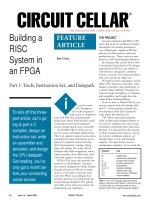
Tài liệu Building a RISC System in an FPGA ppt
... jump and branch- taken take three cycles (no branch Listing 1— This sample C code declares a binary search tree data structure and defines a binary search function. Search returns a pointer ... using a jump. Because insert- ing a jump may make other branches far, we repeat until no far branches remain. Next, we evaluate fixups. For each one, we look up the target address and apply...
Ngày tải lên: 26/01/2014, 14:20

Tài liệu Building a RISC System in an FPGA Part 2 docx
... stage • DCINT: int in DC stage • DMAP: DMA transfer pending • INTP: interrupt pending DCANNUL and EXANNUL are set after executing a jump or taken branch. They suppress any effects of the two instructions ... memory access, causing pipe- line havoc (see Table 3). In t 4 you must run a load data access instead of an instruction fetch. You must stall the pipeline to squeeze in this ac...
Ngày tải lên: 26/01/2014, 14:20
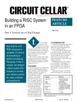
Tài liệu Building a RISC System in an FPGA Part 3 doc
... inter- rupts, insert wait states, and so forth. EXTERNAL RAM The external RAM is a classic 32-KB fast asynchronous SRAM with a 15-ns access time (t AA ). Its pins in- clude A1 4:0 (address), D7:0 (data in/ out), ... make ease-of-use tradeoffs in favor of core users. Because FPGAs are malleable and FPGA SoC design is so new, I wanted an interface that can evolve to address new requi...
Ngày tải lên: 26/01/2014, 14:20